This thread has been locked.

If you have a related question, please click the "Ask a related question" button in the top right corner. The newly created question will be automatically linked to this question.

HD3SS3220: questions about hd3ss3220 UPF EVM SCH

Part Number: HD3SS3220

Hi team,

My customer wants to use HD3SS3220 to develop a MIFI dongle.

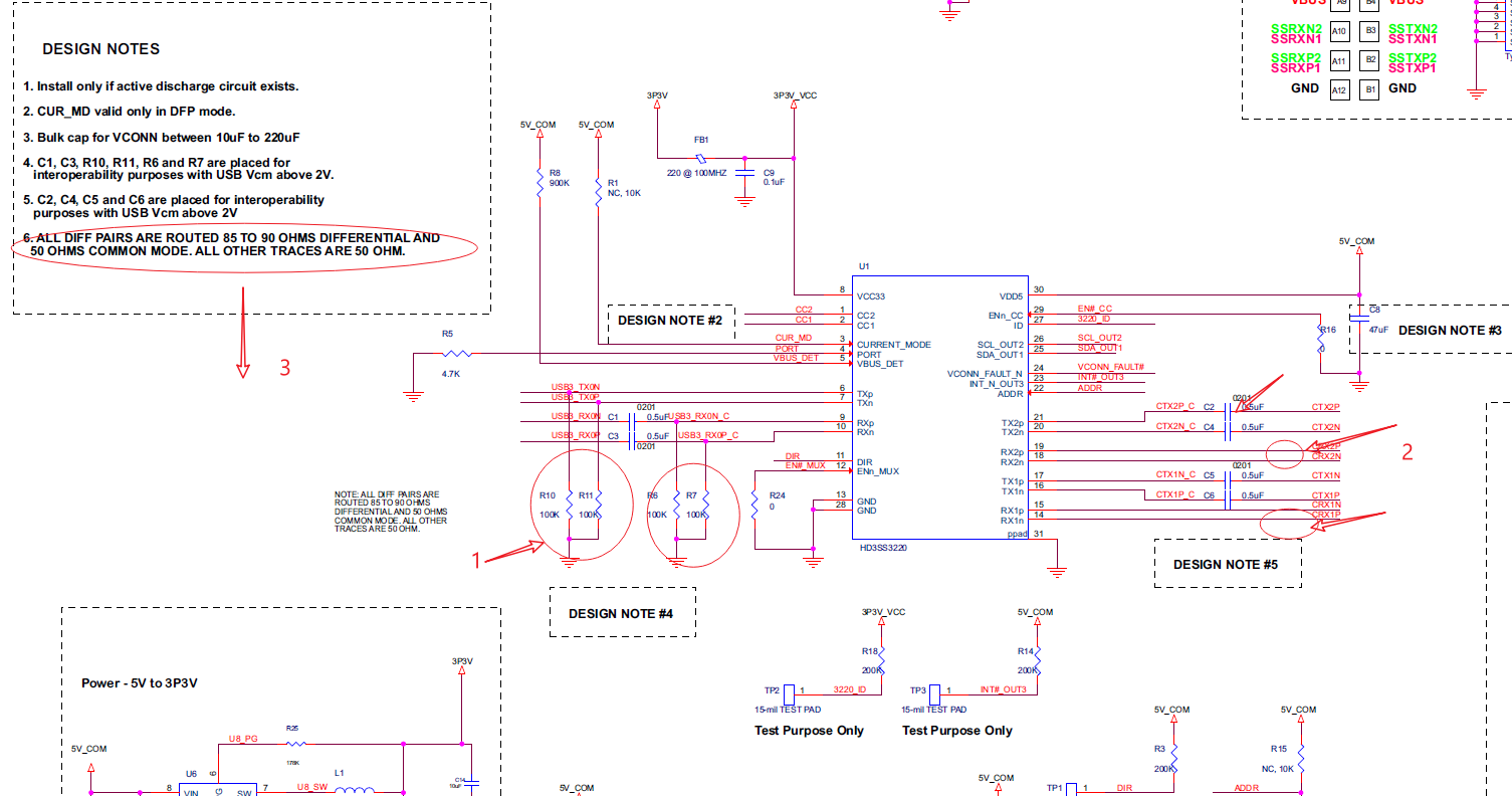
Questions about the HDSSS3220 UFP EVM SCH are:

1. why we put R10, R11, R6, R7 resistor there, customer don't understand the design note#4.

2. there are AC coupled cap on CTX2P and CTX2N, why we don't put AC coupled cap on CRX2P, CRX2N?

3. design note#6 say that DIFF PARIS routed 85-90ohms, 50ohms common mode. Does it mean I need to connect a 50ohms res in each trace?

 Best regards,

Shubiao

  • Hi Shubiao,

    1. Since the internal high speed mux is completely AC coupled on both sides R10, R11, R6, R7 provide DC bias.

    2. AC coupling is allowed on CRX pins. These caps are not included since CRX is connected to the DFP TX which is AC coupled (CRX pins are AC coupled by DFP). Most recent recommendation is that CTX1/2 should be AC coupled with 220nF and CRX1/2 should be AC coupled with 330 nF.

    3. This note refers to the impedance of the PCB trace themselves. 

  • 1: The purpose of 220 kΩ resistors is to discharge the capacitor with in 250ms after a USB device is removed from the USB connector

    2: there should be Ac cap on the other side of TX

    3: no, this is for trace impedance.

  • Brian Zhou said:

    1: The purpose of 220 kΩ resistors is to discharge the capacitor with in 250ms after a USB device is removed from the USB connector

    2: there should be Ac cap on the other side of TX

    3: no, this is for trace impedance.

    1. Does that mean the 100k ohm between TXp and GND is not necessary for the high speed link.

    2. got it.

    3. if the Differential trace impedance is less than required 85-90ohms, i need to put external res to compensate the trace impedance, right?

    Thanks for your feedback.

    Best regards,

    Shubiao

  • 1: these resistors are needed only common mode voltage is >2v

    3: you can not compensate trace impedance by adding additional resistor. Pls read transmission line and TDR related material

  • Hi Brian,

    I found that cc1 pin controls Ch2(TX2 and RX2) and cc2 pin controls Ch1 (TX1 and Rx1).

    However, this is opposite with notebooks type C port.

    1. On customer board, we cannot swap cc1 and cc2 pin connection, is there any method to toggle the “DIR” control logic. if not, would you please advise how to swap cc1 

    2. Is the CABLE_DIR(bit 5 of register 0x09) is the same with DIR pin out?

    Best regards,

    Shubiao

  • 1: TX1/RX11, TX2/RX2 is controlled by DIR pin, not CC1/CC2

    2;  CABLE_DIR(bit 5 of register 0x09) should be  the same with DIR pin out