This thread has been locked.

If you have a related question, please click the "Ask a related question" button in the top right corner. The newly created question will be automatically linked to this question.

DP83869HM: DC-bias voltage at TD_P_B is 0V. No data can be read from PHY register.

Part Number: DP83869HM
Other Parts Discussed in Thread: DP83869, TPS54160

Hi,
I am working with the DP83869HM for a 1000M media converter. I connected the board as follows.
PC-->RJ45-->HX5008NL-->DP83869HM-->SFP Module-->fiber
DP83869 seems not working at all.
(1) PC could not detect the device and said cable is removed.
(2) Clock at XI pin is 25MHz. But there is no output at CLK_OUT. The pin's level is VDDIO. 
(3) I tried to read the register, but retured value is 0xFFFF.
(4) I tested all the four pairs of MDI signal and I can see FLP pulses at all these four pairs. But it is very strange that the DC-bias voltage at TD_P_B and  TD_M_B are both 0V at chip side and transformer side with the other three pairs are 1V. It's not the reason of tranformer or the center-tap capcitor because It is the same when I remove tranformer's Pins or the capcitor. 
(5) RESET and PWR_DN pins(#43 and #44) are pulled to VDDIO with 10k and 2.49k respectively.
(6) RX_D2, LED[2:0] are pulled to VDDIO with 2.49k resistors. This strap configuration means 1000M media converter mode with auto negotiation ( 1000 Advertised) and fiber force mode according to table 12 and table 18.
(7) RBIAS (PIN 12) tied to GND with a 11k resister.
(8) MDC and MDIO are pulled to VDDIO with  2.49k resistors.
(9) The chip is powered in 3-power mode and the power rails are 2.5V/1.8V/1.1V. VDDIO=3.3V.
(10) All the other pins are left open as default.
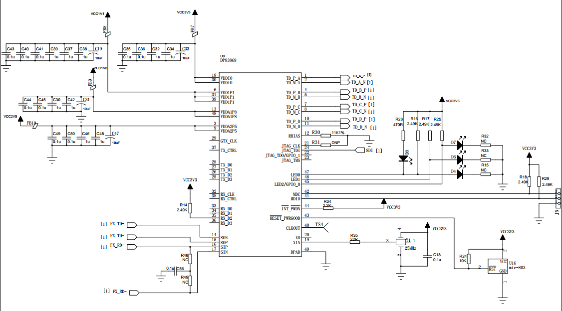
The schematic is as follows.

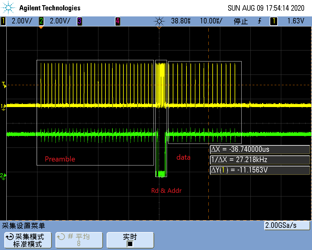
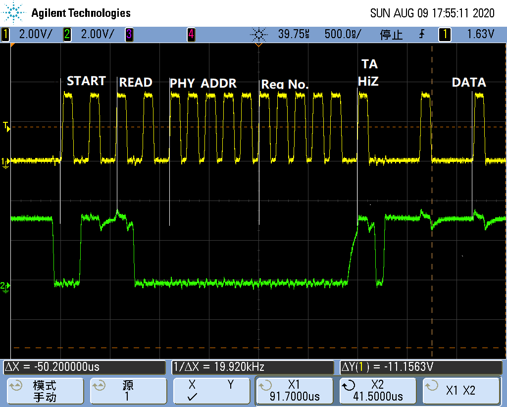
The waveform to read PHY register is as follows. I use MCU's GPIOs to read the register. I'm sure the programe is good and I can use it to read KSZ8041 correctly.

So how I can do next to fix the problem? Thank you!

  • Hi Yansheng,

    Thank you for submitting your question. For point #3 you mention that you tried to read the register and it comes back reading 0xFFFF. Can you confirm which register you are trying to read? 

    Also, can you confirm you have configured the straps to the proper OPMODE as outlined in our app note? https://www.ti.com/lit/an/snla318/snla318.pdf

    Once I have more information about the strapping configurations and the register reads I can help determine what could be the next steps for the debug.

    Thanks,

    Cecilia

  • Hi.

    I read register 0x00 (BMCR) and 0x01 (BMSR) and the retured value are 0xFFFF. I just removed the pull-up resister on Pin MDC and the read value is still 0xFFFF.

    The other most confused issue is that the DC values at TD_P_B and TD_M_B are around 0V but 1.05V at the other three pairs. It seems there's no pull-up to TD_P_B and TD_M_B inside the chip. I think this maybe the ultimost reason.  

    The following is my Strap-Pin configuration which I check with the app-note. I think the Strap-Pins are right. 

    So what can I do next? Thank you!

    PIN No PIN Name STRAP Function PIN STRAP CONNECTION Mode
    35 RX_D2 OPMODE_2 2.49KΩ Pull-up to VDDIO 1000M Media Converter
    36 RX_D3 OPMODE_1 OPEN
    22 JTAG_TDO / GPIO_1 OPMODE_0 OPEN
    45 LED_2 ANEGSEL_1 2.49KΩ Pull-up to VDDIO Copper Auto Negotiation (1000 Advertised), Auto MDIX
    46 LED_1 ANEGSEL_0 2.49KΩ Pull-up to VDDIO
    47 LED_0 ANEG_DIS 2.49KΩ Pull-up to VDDIO Fiber Force mode
    38 RX_CTRL MIRROR_EN OPEN Copper Mirror
    Disable
    32 RX_CLK LINK_LOSS OPEN Link Loss Pass Thru Enabled
    34 RX_1D PHY_ADD[3:2] OPEN PHY ADDR = 0x00
    33 RX_D0 PHY_ADD[1:0] OPEN
  • Hello Yansheng,

    Datasheet specifies that MDIO requires a 1.5k pullup however you are using a 2.49k resistor. 

    Can you please share where you are connecting your MDC and MDIO pins? Are you using an MCU to read and write to the registers? 

    As for the 0V, can you please share the schematic of the magnetics for these 4 channels? I am trying to understand why you are seeing a different voltage for this channel.

    Thanks,

    Cecilia

  • Though pullup resister value is not critical for MDIO, I changed it to 1.5k. But the retured value is still 0xFFFF.

    I did not layout an MCU on my board. I used a 3-pin connector (J5 on the schematic) to  an MCU, on which I use GPIOs to simulate SMI bus to access the phy registers. (R18, the pullup resister on MDC is not installed.)

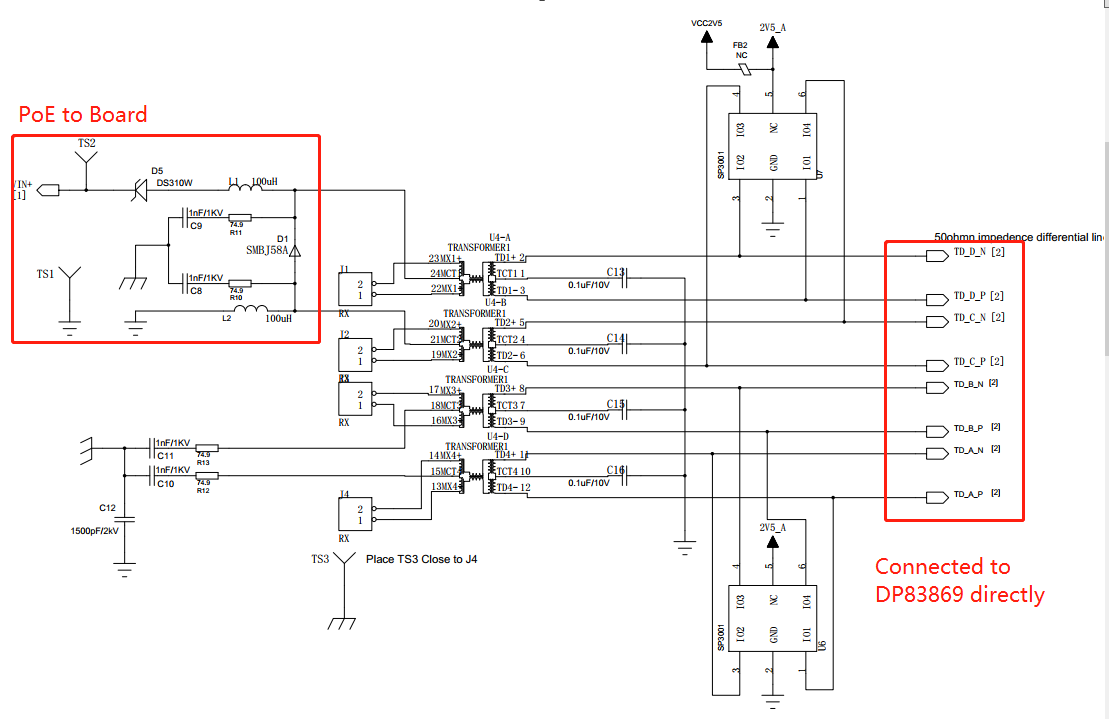
    The magnetics (HX5008NL) and DP83869 schematic are shown as follows.

    By design, the board is powered from two pairs of the cable. So I placed two 100uH inductors and a diode on these two center  taps (Pin #24 and #21) traces. But now I just fed the board with a 12V voltage to the TS2 and then output 3.3V with a TPS54160. So D5, L1 and L2 are not used. I removed all these not-in-used components and TVS arraies (U6 and U7). The DC voltage is still 0V on TD_P_B.

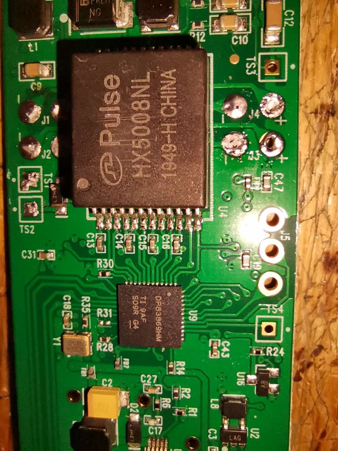
    Would there are any fake chips? I attached the photo of the chip I used. Can you help me to check the mart on the chip? 

  • Hello,

    I will need 1-2 days to verify the board as well as your schematic. I will get back to you on my feedback as soon as possible.

    Thanks,

    Cecilia

  • As for the markings, the device looks to be ok. I will need to verify the schematics and how you are probing the MDC and MDIO lines.

    Thanks,

    Cecilia

  • Hi, is there any progress? Thank you!

  • Hi Yansheng,

    I am sorry for the delay. What is the clock frequency of your MDC that you are using? You also mention that you do not see the 25MHz on the CLKOUT pin is that correct? Can you confirm the specifications of the crystal you are using in your design and make sure it meets the design requirements of our datasheet?

    Thank you!

    Cecilia

  • Hi, I don't know this is or not a good news.

    I found the matter and got it resolved. 

    I made a mistake at clock pins. You know Pin 19 is XO and Pin 20 is XI. But ah ah......the net labels are XI at Pin 19 and XO at Pin 20  in EVM schematic. So I carelessly connected Pin 19 to the oscilator's output and left Pin 20 floating and I used an oscilator instead of a crystal unfortunately. Then you know the last story......

    I took off DP83689 and cropped Pin 19 and shorten Pin 20 to the oscilator's output. Now the good news is that the media converter works well.

    I think it is the net labels in EVM schematic made a mislead. So it is better to edit the schematic next time to comply with datasheet.

    At all, thank you for the advices you gave me these days.

    Thanks! Have a good day!


  • Thank you for sharing. I am glad you were able to solve the issue and I will review your feedback for future changes.

    Thanks and please close this thread.