This thread has been locked.

If you have a related question, please click the "Ask a related question" button in the top right corner. The newly created question will be automatically linked to this question.

DS50PCI402: PCIe Gen2 Link issue

Part Number: DS50PCI402

Dear Technical Support Team,

My application is using backplane with PCI402.

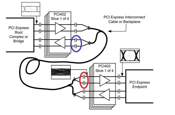
If only AC coupling on the RX side of the endpoint of the backplane is changed to 0Ω resistance
Link up now works properly. (Red circle )

If I change only the AC coupling on the bridge RX side of the backplane to a 0Ω resistor,
There are  the link issue sometimes. (Blue circle)

Can the AC coupling on the RX side be omitted if the backplane length is short?

Best Regards,

ttd

  • Hi,

    Yes, for PCIe only one set of AC coupling capacitors is needed.  The capacitors are almost always on the same board as the PCIe transmitter which is driving the signal.  This is true for any length of PCIe link.

    Regards,

    Lee

  • Hi Lee,

    Thank you for your reply.

    "typical application" of DS50PCI402 I attached the figure, it has the capacitors on both TX and RX side. 

    Could you inform me  this reason?


    Other previous post said "the second pair of AC coupling caps will contribute to signal integrity degradation"

    Maybe, my link up issue seems to related to this.

    ーーーーーーーーーーーーーーーーーーーーーーーーーーーーーー

    https://e2e.ti.com/support/interface/f/138/t/352529

    There is a mistake in this datasheet diagram as it relates to the application. In an active cable (with one DS80PCI102 on each end), the designer will have free choice over the components on either end of the interconnect cable. In this case, only one pair of AC coupling caps are necessary between the two ICs. While including a second pair of AC coupling caps does not necessarily damage the overall system beyond functionality, the second pair of AC coupling caps will contribute to signal integrity degradation, such as lower overall series capacitance and increased signal loss through vias due to routing, since capacitors must be on the top layer and signals could be traveling on middle board layers.

    ーーーーーーーーーーーーーーーーーーーーーーーーーーーーーー

    Best Regards,

    ttd

  • HI,

    The datasheet graphic should be changed.  For PCIe AC capacitors are located on the PCB assembly with the Tx pins.  This convention allows PCIe compliant boards to be connected together and always be AC coupled.

    Regards,

    Lee