This thread has been locked.

If you have a related question, please click the "Ask a related question" button in the top right corner. The newly created question will be automatically linked to this question.

DS90UB933-Q1: DS90UB933-Q1: Signal waveform and communication issues

Part Number: DS90UB933-Q1

Hello

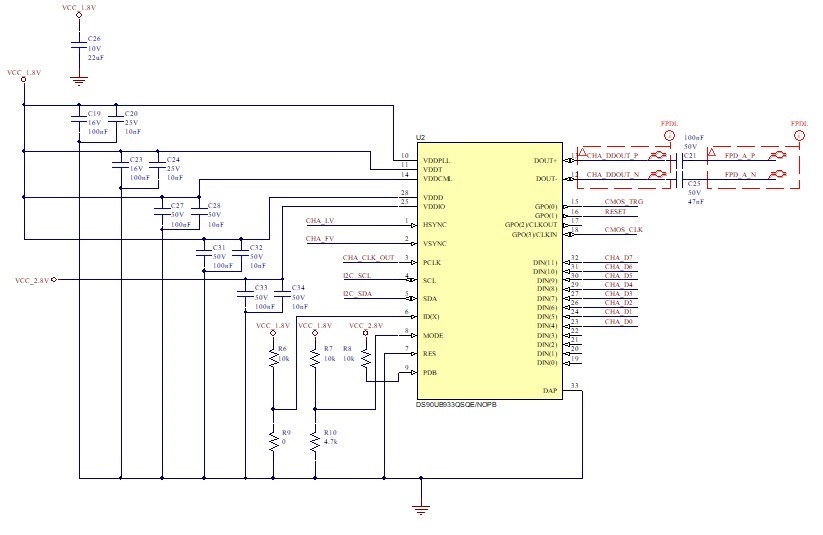
we are debuggin a new project pcb board based on FPDLINK 933 and 934. We are facing some issues in communication.

- 933 side the OnSemi ar0239 and mt9p031 cmos sensor (at 48MHz)

- 934 side a Xilnx FPGA

- using STP cable without POC

- 933 configured to use PIXCLK source from sensor (reg 0x3 set to 0xc3)

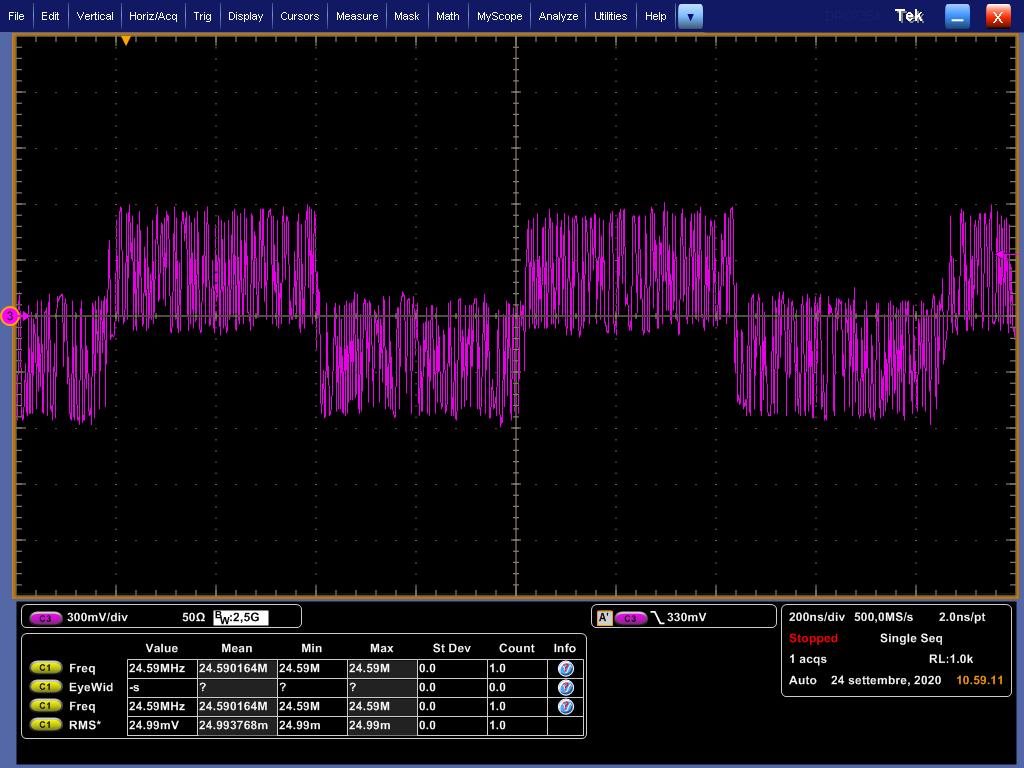
What we see is that sometimes PASS signal goes down for about 2-5 cycles of clock (and of course the stream "jump" with strange image effects). LOCK remains stable. We guess that something is going wrong in the communication path. We start to investigate the signals, and the signal at receiver side is strange. It seems modulated with a frequency of about 1.2MHz, that changes if we change the cable lenght. I attach a screenshot.

What could be the issues? Could someone help us to find what is going on?

Thanks

  • Hi Fabio, 

    For a schematic review, I will respond next monday (9/28). 

    Thanks 

    Sally 

  • Hello Fabio,

    Apologies but we had a slight delay here. Sally is out but will be back in office tomorrow 

    Best Regards,

    Casey

  • Hello, 


    here are my comments from the review: 

    the caps on the DOUT lines should both be 100nF

    PDB has no capacitor, please add 1 uF cap.
    idx strapping is incorrect. R9 should not be 0 ohm, is this a palce holder?
    GP02 needs to be low during power up, so you can tie to gnd with 40 kohm resistor - this will cause power sequencing errors

    scl and sda should have pull up resistor

    recommend 22 uF on VDDCML
    recommend 4.7 uF on VDDT & VDDPLL
    recommend FB on VDDPLL and VDDCML - BLM15HD102SN1D

    minimum pclk for 10 bit mode is 50 MHz

  • Hello Sally

    - I corrected caps on DOUT (now 100nF both)

    - PDB placed a capacitor

    - idx like the table on the datasheet

    - GP02 placed ressitor

    Other thing where placed around the other part of schematic but it's ok. I will use a 12 bit with 48 MHz input PIXCLK.

    BUT...The waveform remains the same, with the strange behaviour described. I can't understand why.

    K.R.

  • Hi Fabio, 

    The waveform looks like the common mode modulation of the back channel, so this is normal. The frequency of the oscillation is ~2.5MHz which is the back channel frequency. 

    After the modifications, are you still experiencing lock issues? 

    Thanks, 
    Sally 

  • I meant "pass", not lock. 

  • Hello Sally,

    thanks for this clarification, I was thinking that it was right because I tried already the BIST and I monitored the 0x57 register and no errors was found. The PASS continues to have a strange behaviour.

    Since I haven't the control of reset pad of serializer (only of the deserializer near the fpga), I do this:

    - Power the system on (Serializer starts, deserializer is keept in reset)

    - Set SER_REG_0x1 to 0x3f (reset all) and wait 500 ms

    - Set SER_REG_0x1 to 0x38 (reset only analog) and set SER_REG_0xD to 0x95 (forse bit GPIO1 to High value, it is the remote reset of the sensor).

    - Set CMOS settings. This will start the PIXCLK to serializer (but all is in reset with REG_0x1)

    - Set the deserializer On, configure it with Channel 1 instead 0.

    - Set SER_REG_0x3 to 0xC3 (force PIXCLK to run PLL)

    - Set SER_REG_0x1 to 0x30 (all out of reset).

    Is this procedure right? Could the PASS be influenced by Jitter of PIXCLK? Did you know if the 933 was tested with OnSemi Ar0239 or similar?

    K.R.

  • Hello,

    can you send me a register dump of the 934? yes, PASS could be influenced by jitter of the PCLK. Pass will not be asserted if there is an error in the payload, so it's possible that the jitter is causing the bits to be improperly sampled. 

    Thanks 
    Sally