


In following scenario:
- Power on the device.
- Its in RMII Master Mode.
- Don’t program any of its registers.
- Connect it to an Active 100M Link.
- Assert its PWRDN pin 3 (drive it Low).
I understand that this will force it into a “Power Down” mode.
But I have following questions regarding this Power Down mode:
Q1. Is it able to detect Link activity by tuning on or blinking LED0/pin4, or does this require a different low power mode? (entered via a SW command?)
In following scenario.
- Power on the device.
- It’s in RMII Master Mode.
- Program its registers to detect Magic Packets and asset a WoL GPIO pin.
- Connect it to an Active 100M Link.
- Assert its PWRDN pin 3 (drive it Low)
Q2. Is it able to detect a Magic Packet and asset a GPIO pin, or does this require a different low power mode? (entered via a SW command)?
The datasheet mentions on Page 21: “DP83825I WoL logic circuit is able to generate a user-defined event through any of the GPIO pins”.
But the only mention in the datasheet regarding how/which pins could be used is in the below:
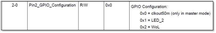
Q3. Does that mean that “any of the GPIO pins” actually means “only pin 2” (50MHzOut/LED2)?
Note that in my application I need two separate LED/GPIO pins for following functions:
- Link/Activity (must be by default; without programming)
- WoL (it’s OK if this requires some programming)
Q4. Do I understand correctly that this is possible with this part, but only RMII Slave Mode (not Master Mode, since that requires using pin 2 as 50MHz Clock out)?
FYR The below table on page 73 of the datasheet is confusing.
I believe the lines that I marked up with yellow highlight below should be deleted from it.

