This thread has been locked.

If you have a related question, please click the "Ask a related question" button in the top right corner. The newly created question will be automatically linked to this question.

DP83869HM: DP83869HM

Part Number: DP83869HM
Other Parts Discussed in Thread: DP83869, DP83869EVM

HI, 

We are using DP83869HM as media converter from Copper to Fibre Converter. We are able to get the Link on both Copper and Fibre side, but we are not able make the communication. 

Please find the attached schematic.

Mode Selection : 1000 Base T - 1000 Base X.

Auto negotiation : Enabled.

We are not using any PHY ID configuration registers.

Can you please let us know if we are missing out some things in the star configuration.media_converter_final_sch.pdf

  • Hi Hemanth,

    If you have register access, can provide a read of the following registers

    • 0x0
    • 0x1
    • 0x9
    • 0xA
    • 0x10
    • 0x11
    • 0x14
    • 0x17
    • 0x19
    • 0x31
    • 0x32
    • 0x33
    • 0x6E
    • 0x1DF

    I will review the schematic and provide feedback by Thursday this week.

    Thank you,

    Nikhil

  • HI Nikhil,

    We do not have access to MDIO registers. We want use DP83869 as media converter using only Strap settings.

    Looking at the forum queries, still I couldn't the clear answer.

    Can we use DP83869 IC as media converter using only boot Strap Settings? Can you please confirm.

    Regards

    Hemanth R

  • Nikhil,

    We were able to read the registers using USB to MDIO dongle, please find the below readings,

    Register 0000 is: 1140

    Register 0001 is: 7969

    Register 0009 is: 0300

    Register 000a is: 7800

    Register 0010 is: 5048

    Register 0011 is: B802

    Register 0014 is: 29C7

    Register 0017 is: 0040

    Register 0019 is: 4444

    Register 0031 is: 10B0

    Register 0032 is: 0050

    Register 0033 is: 0000

    Register 0033 is: 0000

    Register 006e is: 2800

    Register 01df is: 0044

  • Hi Hemanth,

    Thanks for providing the register dump. The schematic, Register 0x6E, and register 0x1DF have all confirmed that the bootstrap setting for 1000Base-T to 1000Base-X mode is correct. For this PHY R81-R85 may be removed, voltage divider is not needed. 

    Initially, you mentioned you are able to observe link on both the copper and fiber side, but register 0x1 is currently showing "no valid link established." How have you confirmed link was established?

    Thank you,

    Nikhil

  • Nikhil,

    Yes, I had mentioned on the link establishment, but it was more to to with the LED. I do not think we have established the link.

    Did you see anything on the schematic which may be causing the issue.

    Do you have any recommendation ?

    Regards

    Hemanth R

  • Nikhil,

    Also, we are able to see the Activity LED on ethernet side. Once you stop pinging from the PC, the blinking stops.

    So my doubt is on the Fibre Connector and Communication levels. Can you please suggest if something has gone wrong at that end.

    Regards

    Hemanth R

  • Hi Hemanth,

    In regards to the schematic, I mentioned that the DP83869HM does not require the voltage divider on the SIP, SOP, SIN, SON pins. However, I made a typo, all resistors R81-R88 may be removed, not just R81-R85. Does link establish correctly once these resistors have been removed?

    Thank you,

    Nikhil

  • HI Nikhil,

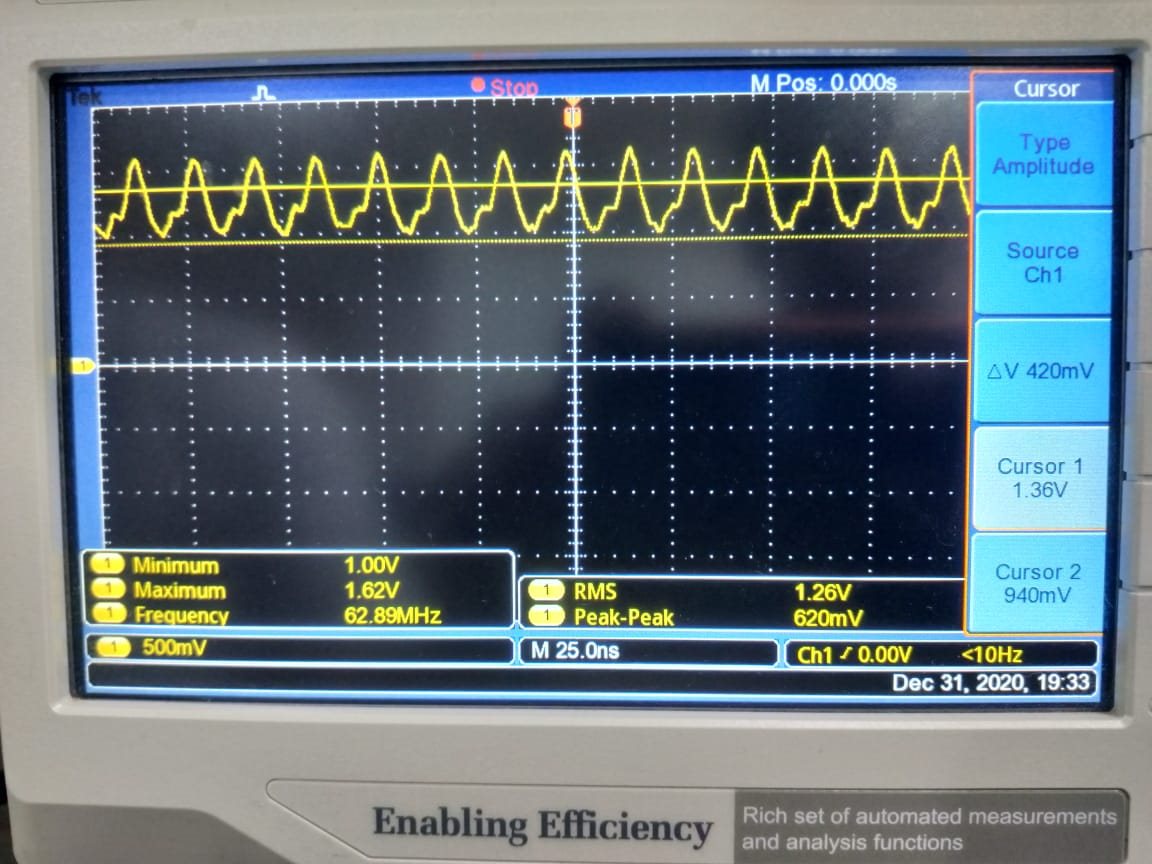
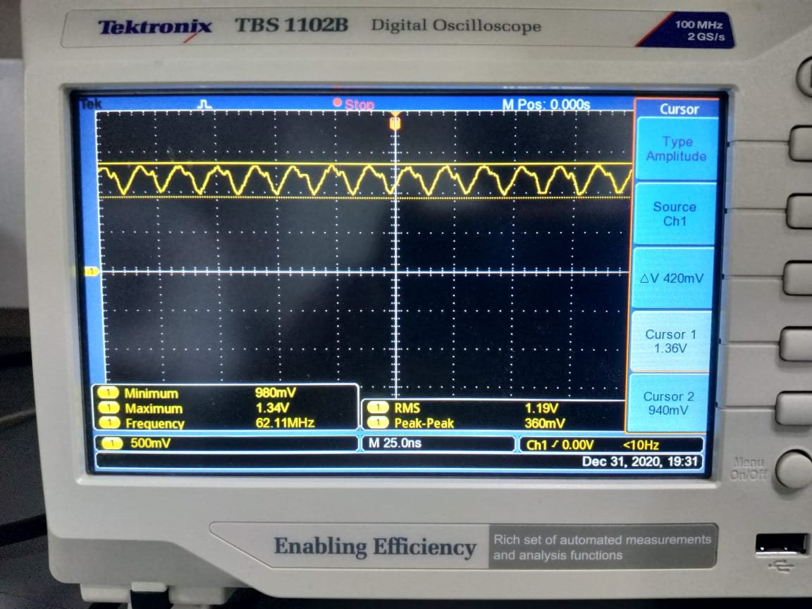
    Yes, we have removed the resistors and also connected Pull-down resistor on Signal Detect pin(After Looking at the suggestion made in Forum discussion). I am able see the signal detect pin going High after connecting the fibre cable. But still I am not able see the link.

    Also, we did probe the signal levels on SI_P and SO_P. Please find the signal level, but we couldn't see anything suspicious.

      Let me know your thoughts on the same.

  • HI Nikhil,

    Did you get a chance to look at the above mentioned issues. 

    Except link we are able to notice all the other changes through the registers. We are not able to find any errors through the register readings.

    Kindly look into the same.

    Regards

    Hemanth R 

  • Hello,

    Thanks for the follow up. Replies on E2E are delayed due to end of year holidays. We will get back to you by Jan 7.

    -Regards

    Aniruddha

  • Hello,

    I have noticed an issue with the DP83869EVM Evaluation board that relates to the SFP connection that you have copied on your schematic.  On the Evaluation board there is a 4.7k ohm resistor, R26, that pulls pin 3 of the SFP (Tx Disable) to ground.  In my experience, there are SFP modules out there that have an internal pull-up resistor of 4.7k to 10k ohms on this pin and so by using this pull-down resistor you are creating a voltage divider which effectively stops the SFP module from transmitting.

    For my design, I simply removed this resistor and have pin 3 of the SFP going straight to ground and this works for all of the SFP modules I have tried it on.

    I would suggest that you replace R70 of your design with a 0 ohm resistor and see if that improves the situation.

    Best regards

    Gareth

  • The SFP module which I have used doesn't have a internal pull up. We must connect a pull down resistor or leave it has NC.

  • Hi Hemanth,

    Can you provide the SFP model part number? Additionally can you provide a read register 0x1 multiple times to check for link, and then provide a full register dump as before, now adding the registers named below?

    • 0xC01
    • 0xC04
    • 0xC05

    Thank you,

    Nikhil

  • Nikhil,

    Please find the below register values and data-sheet of the SFP module, we are not able to understand what might have gone wrong, because except link we are getting all the register values correctly,CS13F-24K-3S-TI-L.pdfCS13F-24K-3S-TI-L.pdf

    Register 0001 is: 7969

    Register 0001 is: 7969

    Register 0001 is: 7969

    Register 0001 is: 7969

    Register 0001 is: 7969

    Register 0001 is: 7969

    Register 0001 is: 7969

    Register 0001 is: 7969

    Register 0C01 is: 7969

    Register 0C01 is: 7969

    Register 0C01 is: 7969

    Register 0C01 is: 7969

    Register 0C01 is: 7969

    Register 0C01 is: 7969

    Register 0C01 is: 7969

    Register 0C04 is: 0181

    Register 0C04 is: 0181

    Register 0C04 is: 0181

    Register 0C04 is: 0181

    Register 0C04 is: 0181

    Register 0C04 is: 0181

    Register 0C04 is: 0181

    Register 0C04 is: 0181

    Register 0C05 is: CDE1

    Register 0C05 is: CDE1

    Register 0C05 is: CDE1

    Register 0C05 is: CDE1

    Register 0C05 is: CDE1

    Register 0C05 is: CDE1

    Register 0000 is: 1140

    Register 0000 is: 1140

    Register 0000 is: 1140

    Register 0000 is: 1140

    Register 0001 is: 7969

    Register 0009 is: 0B00

    Register 0009 is: 0B00

    Register 0009 is: 0B00

    Register 000A is: 7800

    Register 000A is: 7800

    Register 000A is: 7800

    Register 000A is: 7800

    Register 0010 is: 5048

    Register 0010 is: 5048

    Register 0011 is: BB02

    Register 0011 is: AB02

    Register 0011 is: AB02

    Register 0014 is: 29C7

    Register 0014 is: 29C7

    Register 0014 is: 29C7

    Register 0017 is: 0040

    Register 0017 is: 0040

    Register 0017 is: 0040

    Register 0019 is: 4440

    Register 0019 is: 4440

    Register 0019 is: 4440

    Register 0031 is: 7969

    Register 0031 is: 7969

    Register 0032 is: 2000

    Register 0032 is: 2000

    Register 0033 is: A0F1

    Register 0033 is: A0F1

    Register 0033 is: A0F1

    Register 006E is: 0000

    Register 006E is: 0000

    Register 006E is: 0000

    Register 01DF is: F000

    Register 01DF is: F000

    Register 01DF is: F000

    Register 01DF is: F000

  • Hi Hemanth,

    Please allow some time to review register dump and SFP module. We are looking into this issue and will provide feedback by Wednesday of this week.

    Thank you,

    Nikhil

  • Nikhil,

    Also, I checked on the timings for Reset and Power Sequencing. It is as per the Timings mentioned in the Datasheet.

    I strongly doubt on the Voltage levels at the SFP module.

    Can you let us know you suggestions.

    Regards

    Hemanth R

  • Hi Hemanth,

    In this most recent register dump, the values for the registers 0x31, 0x32, 0x6E, and 0x1DF are different from before. Registers 0x6E and 0x1DF no longer show that the PHY is set for Media Converter mode. Are these the correct values? If so, does re-setting or power-cycling return the PHY to Media Converter mode per the strap settings from your schematic? Please keep in mind that these are extended registers.

    If Media Converter mode does not latch in from strap settings after a reset or power-cycle, can you try programming the PHY for media converter mode with the following script:

    • Write 0x0024 to register 0x1DF //media converter mode
    • Write 0x1140 to register 0x0000 //auto-negotiation on copper side
    • Write 0x5048 to register 0x0010 //Auto-MDIX

    Thank you,

    Nikhil

  • Nikhil,

    Please find the below dump. Register Dump looks fine.I do not think it is something to with the bootstrapping registers.

    Did you get a chance to look at the voltage levels at the SFP module, which I had shared.

    I belive somethings is wrong in that Voltage levels, which I am not able to get.

    Looking forward for your response.

    Register 0001 is: 7969

    Register 0001 is: 7969

    Register 0c01 is: 6149

    Register 0c01 is: 6149

    Register 0c04 is: 0020

    Register 0c04 is: 0020

    Register 0c05 is: 0000

    Register 0c05 is: 0000

    Register 0009 is: 0300

    Register 0009 is: 0300

    Register 000a is: 3873

    Register 000a is: 3800

    Register 000a is: 3800

    Register 000a is: 3800

    Register 0009 is: 0300

    Register 000A is: 3800

    Register 0010 is: 5048

    Register 0010 is: 5048

    Register 0011 is: B802

    Register 0011 is: A802

    Register 0011 is: A802

    Register 0011 is: A802

    Register 0014 is: 29C7

    Register 0014 is: 29C7

    Register 0017 is: 0040

    Register 0017 is: 0040

    Register 0019 is: 4000

    Register 0019 is: 4000

    Register 0031 is: 10B0

    Register 0031 is: 10B0

    Register 0032 is: 0050

    Register 0032 is: 0050

    Register 0032 is: 0050

    Register 0032 is: 0050

    Register 0033 is: 0000

    Register 0033 is: 0000

    Register 006e is: 280E

    Register 01df is: 0044

    Register 01df is: 0044

  • Hi Hemanth,

    Thanks for again providing a register dump. The values for register 0x6E and 0x1DF look correct this time for Media Converter Mode. However, register 0x32 seems to have strayed from it's default value. Has this register been written to? Can we return register 0x32 to the default value 0xD0?

    As far as the SFP goes, based on the schematic provided and SFP datasheet, I do not see any issues with the SFP. You have already mentioned R81-R88 have been removed, and the SFP does not have an internal pull on the disable pin and requires an external pull-down to enable the SFP. As Gareth mentioned, a stronger pull or 0ohm resistor may be tried to ensure SFP is not disabled.

    Additionally as a debug step, we can try setting the device for RGMII to Copper mode, to test the copper side of the PHY, and then set the PHY for RGMII to 1000Base-X mode to test the Fiber side of the PHY. This way, we can isolate if the issue is coming from the copper of fiber side. These modes can be set through register writes. Please refer to section 9.4.8 for instructions on how to set RGMII to Copper mode and RGMII to 1000Base-X mode. Please check that link can be achieved across the copper interface, and across the fiber interface in each respective mode. 

    Thank you,

    Nikhil

  • Dear Nikhil,

    Actually we have not written any thing to 0X32, we can write 0x00d0. But it will remain till the next reset.

    As mentioned we did try the RGMII to Copper and RGMII to Fibre approach.

    In RGMII to copper mode we are able to the link up detection, where as in RGMII to fibre approach we are not able to get the link.

    Do you think fibre side is having some issues?

    Register 01df is: 0040 --- RGMII to Copper

    Register 01df is: 0040

    Register 0001 is: 7949

    Register 0001 is: 796D --- Link UP

    Register 0001 is: 796D

    Register 01df is: 0041 RGMII to Fibre 

    Register 0c01 is: 6149 --- NO Link.

    Register 0c01 is: 6149

    Register 01df is: 0044 -- No Link.

    Register 01df is: 0044

    Register 0001 is: 7969 -- No LINk.

    Register 0001 is: 7969

    Also, what we noticed on LED1 was, the you enable Media converter mode and RGMII to fibre. We are able to see it LED oN. LED1 pin goes HIGH.


    Type a message

  • Hi Hemanth,

    I see in the schematic, the SD pin of the SFP is routed to both JTAG_TDI and this "SD_FX" signal. The "SD_FX" signal only appears at this point on the schematic provided. Is this signal routed elsewhere?

    Thank you,

    Nikhil

  • Hi Nikhil,

    SD pin from SFP is directly going to JTAG -TDI , no where else in the schematic.

    SD_FX is just a net name.

    Regards

    Hemanth R

  • Hi,

    I think it's the issue of SD signal level.

    SD signal is logic '1', i.e. output high level in normal operation, which is showed in page 4 of SFF module's datasheet. But for the JTAG_TDI of DP83869, when used as signal detection input, is low valid. So I think you should invert the fiber module's SD signal and then feed to JTAG_TDI input.

    Generally, SD is high output for SFF module, but low for SFP module(named as LOS in SFP). The module used for EVM board is an SFP one, which can be connected to DP83869 directly. It should be inverted for an SFF module connected to DP83869.

    You can try to tie JTAG_TDI to ground if you can not add an inverter.

    I hope this can help you!

  • Yansheng,

    Thank you for your response. Yes it solved the issue. It was a logic issue on SD PIN.

    Regards

    Hemanth R