Replies: 14
Views: 91
Part Number: TDP158
Hello, I have a design that interfaces with a camera to an FPGA. I want to display the camera video to an HDMI monitor. I'm looking at the TDP158 and need to know if I need to take care of the EDID? Dos the device have an embedded EEPROM to store the EDID data? This is my first HDMI design.
Thank you
Joe
The TDP158 is a redriver, it does not have stored EDID data. If the FPGA is the sink, then the EDID needs to be stored in the FPGA.
Is the camera output a DC-coupled HDMI or AC-coupled HDMI?
Thanks
David
In reply to David (ASIC) Liu:
Hi David,
I am interfacing with an SDI camera and using the LMH1297RTVT and using an SDI Receiver IP on the FPGA. Is there a web site where I can find the EDID data, some kind of software that can generate this EDID data? 3065872. How do I read the monitor's EDID parameters?
In reply to joe306:
Are you trying to interface a FPGA HDMI Transmitter and a HDMI monitor? I am sorry that I thought you are trying to interface the camera and FPGA through the HDMI interface.
If you are trying to interface a FPGA HDMI transmitter and a HDMI monitor, the EDID information is already present inside the monitor. The FPGA has to use the DDC bus to read the EDID from the monitor. Different monitors will have different EDID to reflect the difference in the manufacturer, resolution, etc. The DDC bus uses the same protocol as the I2C bus. So the FPGA needs to implement the DDC primary function in order to read the EDID from the monitors.
David,
HI, I have been looking a Zynq Ultrascale+ MPSOC Dev Kit that has HDMI TX and they are using the SN65DP159 ReTimer. Like I said, I'm a newbie here and without your comments and looking at Dev Kits I'm lost. Which device is most practical in what I am doing? Could I make things easy by only supporting 1920x1080p at 60Hz resolution and timing? Is the DDC bus on the ReTimer or ReDriver?
Would you please accept my friendship request and maybe we can have a call to go over your questions?
Hi David. I accepted the request.
HI, I the SN65DP159 the SCL_SRC and SDA_SRC I believe is the inteface where the DDC bus can be read.
The TDP158 can either snoop the DDC bus (no 5V to .3.3V level shifting) or provide the 5V to 3.3V level shifter function between the source and the sink DDC bus.
When the TDP158 provides level shifting function, the FPGA issues a DDC read request to the TDP158 SDA_SRC and SCL_SRC at 3.3V, the TDP158 then level shifts the read request to 5V and sends the request to the sink. When the sink returns with the requested data, the TDP158 again pass the requested data from the sink to the source.
Hello, here is what I have so far.
VIB 21.pdf
Joe,
On the schematic
1. Since you are using the TPD12S016, you may want to remove the TPD4E05U06QDQARQ1 ESD protection on the main link and use the TPD12S016 on the main link.
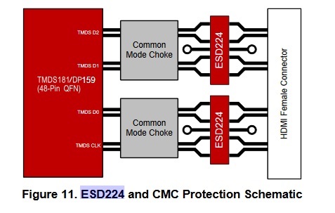
2. Please add HDMI common mode choke on the output
3. You can remove the EEPROM on the CTL_SDA and CTL_SCL and use the FPGA I2C primary to control the DP158/159