This thread has been locked.

If you have a related question, please click the "Ask a related question" button in the top right corner. The newly created question will be automatically linked to this question.

DS32EL0421: Serializer / deserializer pair not locking

Part Number: DS32EL0421
Other Parts Discussed in Thread: DS32EL0124

Hello,

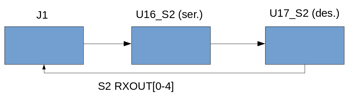
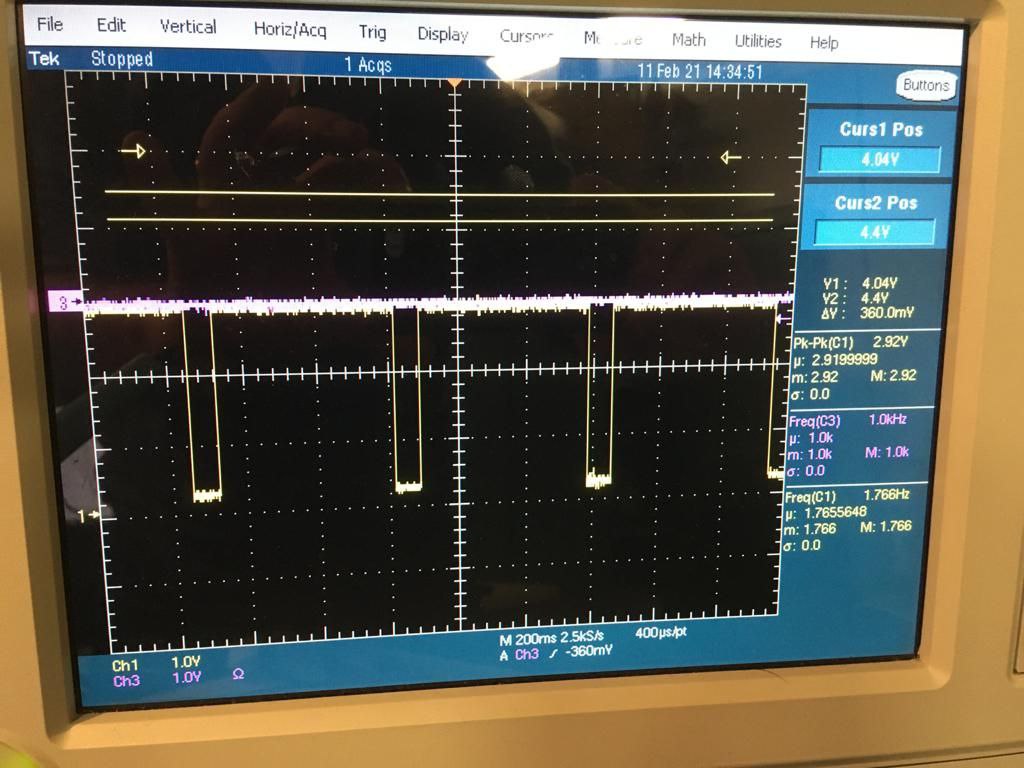
We have designed a custom PCB board featuring a serializer (DS32EL0421) and a deserializer (DS32EL0124). We send a 160 MHz clock to the serializer chip, which however does not seem to lock onto it (the "not lock" pin is at "1"). We use the configuration with remote sense and DC balance enabled.

Please find attached the schematic of the board. Note that in order to test the board we connected the serializer output to the deserializer input. Do you spot any flaw in the design?

Thank you for your attention
Kind regards,
Pietro Carra

MRX_v2.0-SCHEMI_2021.01.13.pdf

  • Hi Pietro,

    The signal path in your schematic is a bit difficult to follow. Can you share a simple block diagram of your system for better understanding?

    It looks like you have 4 EL0421 serializers but only 2 different EL0124 deserializers. It also looks like 2 of each of the serializers are sharing all of the same nets, while both deseriailzers are sharing all of the same nets. Is this the case?

    Regards,

    I.K.  

  • Dear Anyiam,

    Sorry if the schematic is unclear. Please find attached a picture representing our testing conditions.
    It is true that the board holds 4 serializers and 2 deserializers, because it is supposed to communicate with another board with 4 deserializers and 2 serializers. However, for testing purposes, we connected the U16_S2 serializer to the U17_S2 deserializer (they are at pag. 2 of the schematic).
    The serializer input comes from the J1 connector, and the deserializer output should come out of the same connector. However, we observe that when we correctly give inputs to the serialzier, we do not see a corresponding signal on the deserializer. Also, probing the serializer outputs, we do not see any signal transition.

    Thank you for your help,
    Pietro Carra

  • Hi Pietro,

    Unless I'm misunderstanding the schematic, the main issue I see here is that U16_S1 and U16_S2 serializers share all off the same nets. This will cause contention issues. The same can be said about U18_S1 and U18_S2, as well as U17_S1 and U17_S2.

    Regards,

    I.K.  

  • Hi,

    No that is not what happens (if you are referring to page 1 and 2 being the same). It is just a way to have the same schematic for the two groups of serializers.

    The real signal nets are the ones reported in the two green boxes at page 3, which are named at page 1 and 2 according to what is reported in the boxes. So for example the outputs of U18_S2, which are called TX_B_OUT_N/P at page 2, are actually called S2_TX2_OUT_N/P in the rest of the schematic, as reported in page 3 (not conflicting with U18_S1 outputs, called S2_TX1_OUT_N/P).

    I hope this clarifies the misunderstanding.

    Kind regards,

    Pietro Carra

  • Ah okay I understand.

    It's strange that you're not seeing any signal transition on the serializer output. Is it just stuck low/high?

    Can you share waveforms of the LVDS inputs on the serializer? Additionally, are you able to measure how much current the serializer is consuming from the supply?

    Regards,

    I.K. 

  • Hello,

    Sorry for the delay. We tried to measure the ser-des power consumption but it was impossible since many other components share the same power lines. The only thing we can say is that they each draw about 25 mA when they are not receiving the clock and the data. About the input signal waveforms, you can find one attached (in the picture there is one of the two LVDS pairs).

    We also tried to read and write the registers with the I2C protocol. In particular we see that the serializer "sees" a link. We can say this because the register 0x2A reads 00001011, with the last two bits meaning "LINK DETECTED", if I correctly understand the documentation. However the "not lock" pin of the serializer is still high. In which conditions is this pin supposed to go low?

    Do you have any suggestion to troubleshoot the issue? Consider that now we can both read and write to the i2c registers of the serializer and the deserializer.

    Kind regards,
    Pietro Carra

  • Hi Pietro,

    Link detection is not possible without a lock first, as the device will not enter the link detect state until the PLL of the serializer has locked onto the input clock, in which case the /LOCK pin will go low. Do you see this pin toggling between high and low, or register 0x2A toggling between link detected and link not detected? Can you provide a full register dump of all the registers?

    Additionally, if you toggle the /RESET pin do you see any improvement in the issue? Please also ensure the input LVDS clock meets the electrical and timing specifications in the datasheet, and the noise on the power supply is less than 100 mvpk-pk.

    Regards,

    I.K.

  • Hi,

    I see the /LOCK pin constantly high, no toggling. The register instead is constantly at 1. We tried the software reset but it did not help. We still see the same problem.

    The input and clock signals meet the LVDS specifications.

    Please find attached the register dump of the ser/des pair and a picture of the noise on the power line. It is slightly above 100 mv, could this be the issue?

    Regards,

    Pietro Carra

    register_dump.txt
    #N_REGISTER     #OUTPUT
    
    
    #SERIALIZER
    00  10101110
    01  00000000
    02  00000101
    03  00000101
    04  00000100    
    05  00000000
    06  00000000
    20  00000000
    21  00000000
    22  00000000
    24  00000000
    26  00111111
    27  00000000
    28  00000100
    29  00011000
    2A  00001011
    2B  00000000
    2C  00000000
    2E  00000000
    2F  00111000
    30  01100010
    69  00000011


    #DESERIALIZER
    00  10110000
    01  00000000
    02  00000101
    03  00000101
    04  00000100
    05  00000000
    06  00000000
    20  00000000
    21  00000000
    22  00000000
    27  00000000
    28  00101000
    2B  00000000
    2D  00000000
    2E  00010000
    2F  00000000
    3B  01110000
    3D  00000000
    3E  00000000
    3F  00000000
    49  00010110
    60  00000000
    61  00000000
    63  11100000
    67  00000010


  • Hi Pietro,

    Sorry for the delay. The register dump indicates that the serializer sees and detects TxCLKIN, but it's not able to lock for some reason. This may be due to signal integrity issues with the clock or issues with the VDD supplies. Upon power-up, do all of the power rails start at 0 V and monotonically ramp to their final values? Is the input clock provided after the power rails are stable at their final values? Are you able to reduce the noise on the power rails?

    Regards,

    I.K. 

  • Hi,

    We made further tests on the board. We tried to read the GPIOs, and we noted that:

    - GPIO 1: pll lock indicator is high

    - GPIO 2: always on clock is 10 MHz, parallel to serial clock is 80 MHz, digital clock out is stuck low

    The event counters in the register are all 0 except for link counter which is 1. This happens with the serializer receiving a 160 MHz clock, the /LOCK pin is always high.

    We also checked better the power rails and we noticed a 50 KHz frequency noise (see picture) on the 2.5 V rail. This comes from the serializers/deserializers, since there is nothing else on that power rail and if we use the same power chip to power a resistor load we do not see the noise. We do not see this noise on the 3.3 V rail.

    Regarding your questions: the power rail ramp up monotonically and the clock is provided after power up.

  • Hi Pietro,

    The amplitude of that noise does exceed the datasheet recommended condition - are you able to reduce it? Also, does increasing/decreasing the frequency have any effect?

    Regards,

    I.K. 

  • Hi,

    We reduced the noise on the power rails down to 80 mV, but with no improvements.

    We tried different frequencies and we noticed that with a 125 MHz frequency the /LOCK pin was toggling between 0 and 1 as in the picture.

    We tried disabling the remote sense functionality by writing in the registers 0x21 and 0x22 first in the serializer and then in the deserializer. The /LOCK pin of the serializer went down but the one of the deserializer did not. Do you think this means something or is it the normal behavior of the /LOCK pin when the remote sense is disabled?

    Do you have an evaluation board or a reference circuit that shows how to connect these two chips together that we can check?

    Regards,

    Pietro

  • Hi Pietro,

    Very sorry for the delay. When you turn remote sense off and the serializer locks, are you now able to see activity on the output of the serializer? 

    When remote sense is disabled and DC balance is enabled, the Data Valid input to the serializer must be held high for 110 LVDS clock periods. Additionally, an external device should toggle the Data Valid input to the serializer periodically to ensure constant lock. We don't have an EVM for this device but the connections on your schematic look fine (assuming the serializer and deserializer are directly connected with no active components between them).

    It's interesting that you're seeing periodic locking at lower frequencies though. Does your input clock meet the LVDS Timing Specifications listed in the datasheet? 

    Regards,

    I.K.