This thread has been locked.

If you have a related question, please click the "Ask a related question" button in the top right corner. The newly created question will be automatically linked to this question.

ISO5500: query of external buffer circuit with ISO5500

Part Number: ISO5500

Hiii,

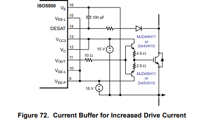
           I am designing a IGBT gate driver with Texas IC  ISO5500 . In my application I require higher sourcing and sinking currents, thats why i am using a external current buffer , same was attached . This circuit was 

suggested in the ISO5500  datasheet, page no.34. when  analyzing the  buffer circuit  , I am getting a voltage  VEB of more than 25V across npn transitor , when below pnp transistor is in operation . But the datasheet  value of VEB for the transistor is 5V only, means it will fail. Same problem for PNP transistor also , when NPN transistor is in operation. please solve my query. Let me know if anything is required.

7563.iso5500.pdf

  • Hi Naga,

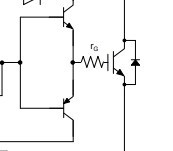
    Thanks for reaching out. The circuit below can help solve the problem. You can also move the gate resistors between BJT collectors and power supply rails. 


    We would recommend ISO5452 which has similar functions as ISO5500 for new designs. 

    Please let us know of any concerns. 

    With Regards,

    Xiong

  • Hiii Xiong,

                       First of all i want to know whether my analysis of the circuit is correct or not which i have mentioned in my earlier post . If  it is correct how TI is recommending the circuit in its data sheet ( ISO 5500, page no 34).  My application requires a external current buffers  with different Rgon & Rgoff resistors, which is not possible with the circuit that u recommended & i don't want to use a diode in series with Rgoff resistor to use the recommended circuit for different Rgon & Rgoff resistors.  My application is IGBT gate driving & the driver IC should work with Bipolar supplies ( +15V & -10V).What extra features have for ISO5452 when compared with ISO5500. 

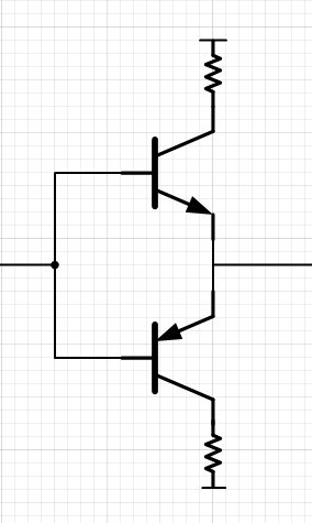
    Note : can u please explain the circuit analysis of  below circuit, especially the voltage across emitter to base of NPN transistor when PNP transistor is in operation &  voltage across  emitter to base of PNP transistor when NPN transistor is in operation. If possible with waveforms.

  • Hi Naga,

    Here is the circuit i meant. This circuit can support separate turn-on and turn-off resistors. 

    ISO5452 is our latest offerings of isolated gate driver with enhanced isolation performance and higher CMTI.

    For the figure 72, the reverse VBE voltage can be as high as (VEE2-VCC2) due to BJT transition time. However, the voltage only lasts for limited time.  

    With Regards,

    Xiong