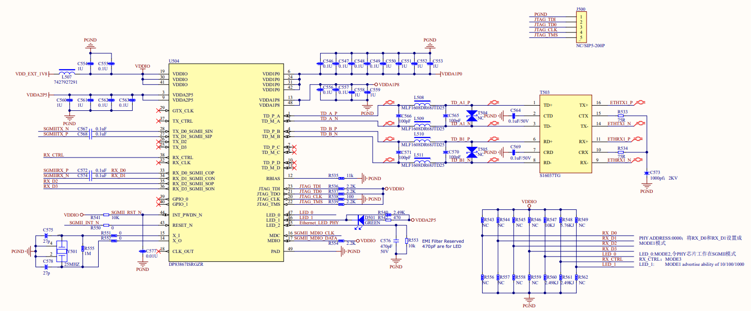
Attached is the dp83867 application circuit I drew. Please help me check if there are any mistakes in the circuit design. Thank you!
I want to configure this chip to sgmii mode, set the transmission rate to 10 / 100 / 1000, PHY address to 0000
The main questions are as follows:
1. Several strap pins default the pull-up and pull-down of internal resistance;
2. Whether there is a STARP pin missing configuration;
3. The power supply of the chip is as follows:
1.0V power supply: continuous power supply current of 300mA;
2.5V power supply: the continuous power supply current is 150mA;
1.8V power supply: 1.8V power supply (50mA) output by 4G module