This thread has been locked.

If you have a related question, please click the "Ask a related question" button in the top right corner. The newly created question will be automatically linked to this question.

DP83867E: Schematic Review

Part Number: DP83867E

Hi ,

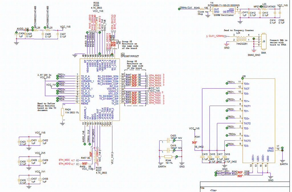
We are using the DP83867 in RGMII configuration for 1000m operation. I was wondering if the TI team can review our schematics and give us feedback on potential issues.

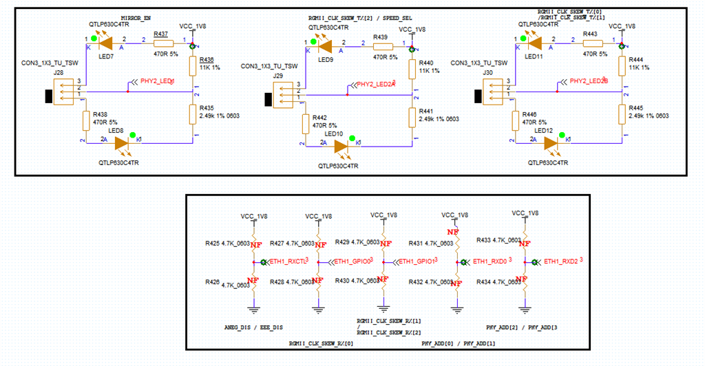
I have also added a provision for the strap pins. I wanted to double check if its possible that the software team can write to the registers and overwrite the default strap configuration after start up?

Regards,

Tony

  • Hello Tony, 

    Thank you for reaching out. I will provide my inputs by the end of this week.

    Regards,

    Sreenivasa 

  • Hello Tony, 

    Please see below comments

    Functional section

    Observations

    MDI interface

    Did you consider ESD protection for the MDI inputs?

    RGMII interface

    The transmit signals terminations have to be placed near to the host.

    Clock :

    Oscillator. Place the smallest vale cap nearer to the oscillator supply pin

    Clk_125MHz

    Take care of routing this signal. Will impact radiated emission.

    INT/PWDN_N

    Check the net connection if used

    GPIO_1, GPIO_2

    Recommend using 2.2kΩ for improved noise performance

    /PHY_RESET0@G

    Please take care of power-up and reset timing

    MDC, MDIO

    MANAGEMENT DATA I/O: Bi-directional management instruction/data signal that may be sourced by the management station or the PHY. This pin requires pullup resistor. The IEEE specified resistor value is 1.5kΩ, but a 2.2kΩ is acceptable.

    JTAG clock termination

    Consider terminating the JTAG signals as per the EVM

    LED8, LED10, LED12

    Pull up strap resistor value. Please refer to 4-Level Strap Resistor Ratios of the datasheet

    Power supply Decap

    VCC_2V5 (VDDA2P5 – 2)

    Recommend to use 2 X 0.1uF connected nearest to the pin  + a single 10uF cap + 10nF (connected close to the 10uF)

    AVDD_1V8 ( VDDA1P8 – 2 pins)

    Recommend to use 2 X 0.1uF connected nearest to the pin  + a single 10uF cap + 10nF (connected close to the 10uF)

    VCC_1V8 ( VDDIO - 3 pin)

    Recommend to use 3 X 0.1uF connected nearest to the pin  + a single 10uF cap + 10nF (connected close to the 10uF)

    VCC_1V1( VDD1P0 - 4 pin)

    Recommend to use 4 X 0.1uF connected nearest to the pin  + a single 10uF cap + 10nF (connected close to the 10uF)


    Power sequencing

    When operating in three-supply mode, the 1.8-V VDDA1P8 supply must be stable within 25 ms of the 2.5-V VDDA2P5 supply ramping up. There is no sequencing requirement for other supplies when operating in three supply mode.

    For DP83867, two things cannot be changed via software. All other changes are possible via software.

    1. PHY address
    2. If auto-negotiation is disabled via strapped then it cannot be enabled through software. But if it is enabled via strap then it can be disabled via software.

    Regards,

    Sreenivasa 

  • Thanks Sreenivasa. I will incorporate your suggestions.