This thread has been locked.

If you have a related question, please click the "Ask a related question" button in the top right corner. The newly created question will be automatically linked to this question.

TCA9539: Asking for the TCA9539 output spec and the level shift

Part Number: TCA9539
Other Parts Discussed in Thread: TXB0108

Hi team,
Customer would like to use two TCA9539 on the project.
Please help for the three questions.
1. one of TCA9539 VCC is 1.8V. However, cusomter measure the voltage test point TP4588 which connect to P06 pin10.
TP4588 voltage is 3.8V. does that make sense the I/O port's voltage is higher than VCC 1.8V?

2. the second TCA9539(U4501), several GPIO connect to TXB0108 for 3.3V to 5V level shift.
Could you please review the schematic is ok or not?

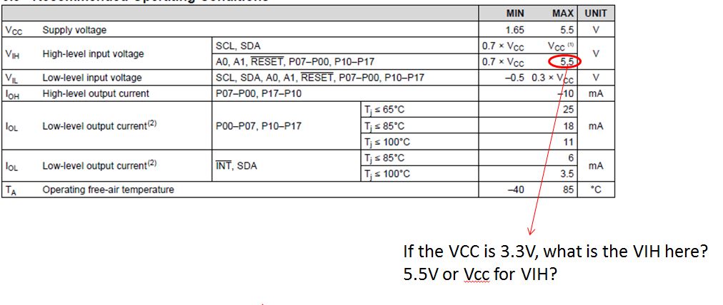
3. for the user case VCC is 1.8V, according to the spec, the max VIH is 5.5V for the P07-P00. Is that right? or the max should be VCC instead?


Thanks,
SHH

  • Hi SHH,

    Thank you for reaching out.

    1. Due to the fact that the device is powered by 1.8 V a higher voltage must come from outside connected on the P06 pin10. This could be wanted or not - it depends on the application. Maybe its possible to get more information about the system to clarify this. For sure I can say that this voltage is not harming the device its capable to handle up to max 5.5 V on P00 ... P17 but double check as I mentioned to make sure there is not an excessive amount of current going into the pin.

    2. As far as I can tell the schematic and the connections to the level-shiftier looking correct it is pretty straight forward.

    a. The only thing I can point out is that you could realize the 5 V levels at the TCA9539 pins P00 ... P17 by adding a pull up resistor to a 5 V rail but if the system works with the level-shifter there is no need to change anything.

    b. Make sure that the I/O  P00 ... P17  pins are always defined, adding a pull up to Vcc or pull down to GND to set a default state

    c. Also put a pull up resistor on the INT pin otherwise it will be nevver chane the LOW state after it got pulled down

    3. The max V_IH is always 5.5 V independent from what Vcc is applied on the device - same as described as in 1.

    I hope this is helping you out, let me know if there is anything else I can do!

    Kind regards 

    Dierk