This thread has been locked.

If you have a related question, please click the "Ask a related question" button in the top right corner. The newly created question will be automatically linked to this question.

TCA9548A: VCC for a 1.8V master

Part Number: TCA9548A

Hello,

I have a question about the appropriate VCC on TCA9548A with a 1.8V master and 3.3V slaves. VCC is 2.5V. I used Example 2 in the post below to set this voltage.

e2e.ti.com/.../636174

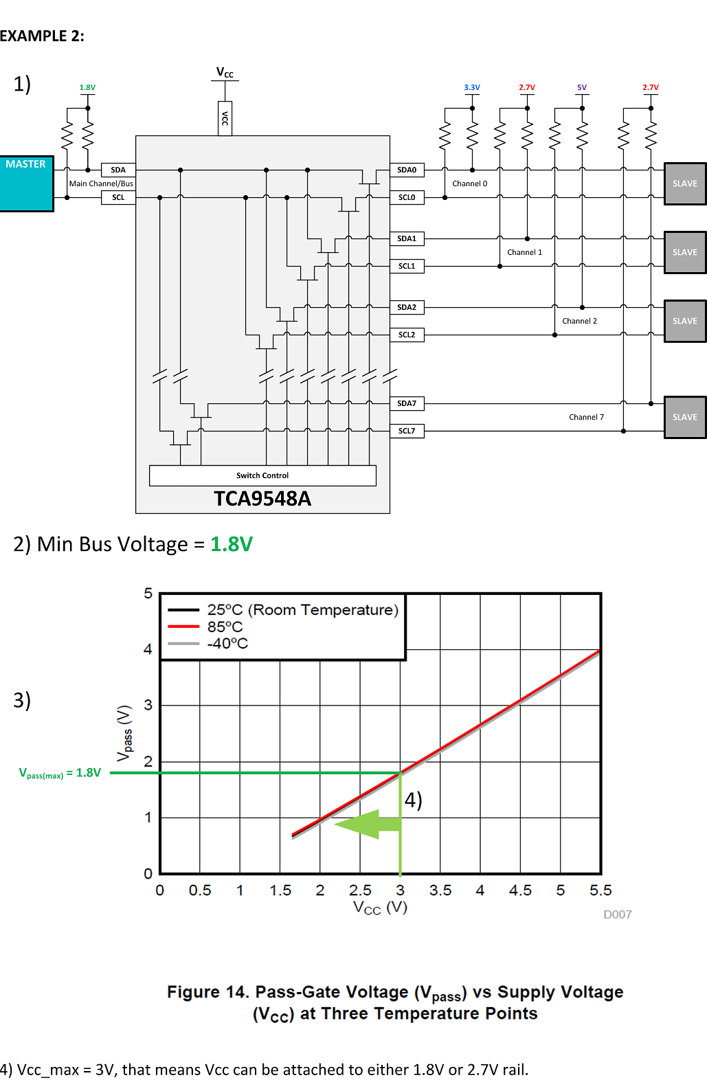
It is my understanding 2.5V would be fine. However while reviewing the design, I found Vih to be 0.7 x Vcc (Table 6.3 of the data sheet) for A0-A2, SCL, SDA and /RESET.

Now, 0.7 x 2.5V is 1.75V which is too close to the master's 1.8V.

For one, I would like to know what I am missing in this analysis.

On the other hand, I would like to know if there is any performance penalty if I set VCC to 1.8V, as it would allow me to eliminate a level translator (1.8V > 2.5V) for the /RESET line.

Thanks in advance.

  • Hey Elder,

    "For one, I would like to know what I am missing in this analysis."

    Your analysis is correct, the main bus with a 1.8V pull up is very close to the device's ViH. With a strong pull up resistor you could make this work.

    At 3V Vcc which you worked out from the earlier example, the ViH would not be met with a 1.8V. The 3V maximum you calculated is to ensure the pass FET between the main channel and the accessory channels do not partially conduct. (If this happened then the pull up voltage on all the channels would be pulled down slightly). I ran through an example of this in simulation here:

    "On the other hand, I would like to know if there is any performance penalty if I set VCC to 1.8V, as it would allow me to eliminate a level translator (1.8V > 2.5V) for the /RESET line."

    Making the Vcc = to 1.8V will mean it takes a little bit longer for a low to pass from one side to another. So essentially it will generate a minor propagation delay from a transition of high to low.

    The reason here is the gate voltage at 2.5V (Vcc) and a threshold voltage (Vth) at lets say 1V means that a channel (main or accessory) needs to pull down to atleast 1.5V because the opposite side begins to pull down.

    Redo this example with gate voltage at 1.8V (Vcc) and the same threshold voltage. This example the pull down voltage is 0.8V before the signal on the other channels will start to pull down.

    The difference in these two examples is 0.5V which when you pull down is very quick (nano second range). The only other thing I can think of is because the gate voltage is lower, we will see a larger Rds (impedance between the channels) which won't really cause any issue unless you are pairing this with a buffer with a static voltage offset connected to once of these channels.

    Thanks,

    -Bobby

  • Hello Bobby,

    First of all, thank you very much for your fast response.

    About the first answer, are those examples taken from an application note? If affirmative, then the app. note should be corrected as it induces the user to error. In my use case it would marginally work but if one followed the 3V or even 2.7V VCC, they would not be using the part by the specs.

    Regarding the second answer, I am not sure I fully follow you but I will dig deeper into it. Anyway it seems in my case suplying the IC with 1.8V is the way to go. I may even reduce SCL to 100kbps if I need.

    Thanks again.

    Elder.