This thread has been locked.

If you have a related question, please click the "Ask a related question" button in the top right corner. The newly created question will be automatically linked to this question.

UCC21520: gate driver output waveform not good

Part Number: UCC21520

Hi, my customer is using UCC21520 to drive a single phase full bridge AC/DC PFC consists of 8 MOSFET(each leg two MOSFET in parallel), each UCC21520 drives one half bridge. Right now they are only switching the low side of the half bridge, the high side is always kept low. The schematics are as below.

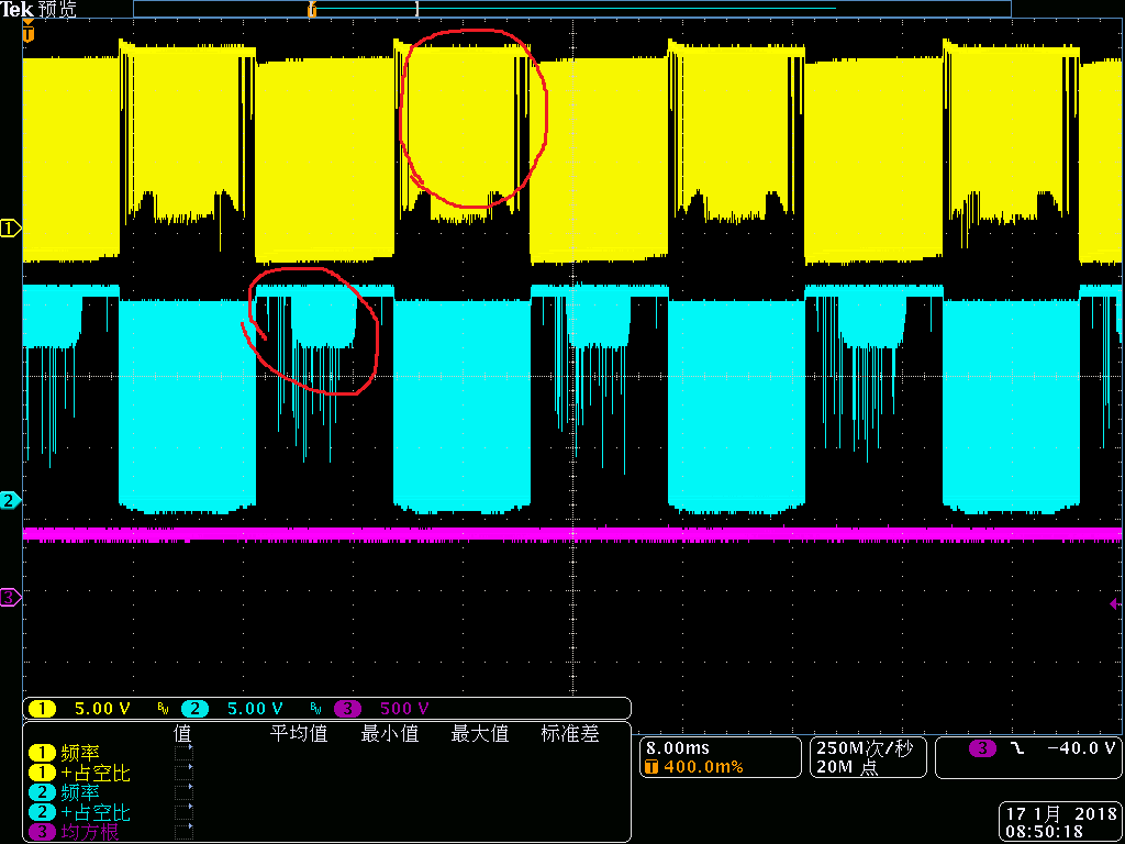
The waveform is as below, the yellow one is the low side MOSFET G-S waveform of phase L half bridge, blue one is the low side MOSFET G-S waveform of phase N half bridge. Since the AC input is 50Hz, 20ms period, each low side should be in high frequency switching mode for 10ms, and be constant high for the other 10ms. We can see that there are a lot of oscillation when the low side MOSFET gate side should be kept high (red circle part in the picture below).

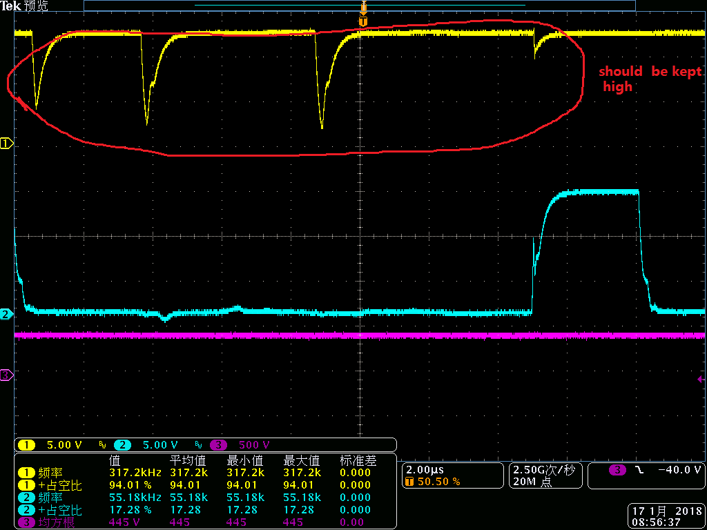
By zooming in, we can see the waveform like:

1. what may cause the spike(or oscillation?) of the G-S waveform and how can we decrease it?

2. For the blue waveform in the picture above, the miller platform is very obvious and the yellow waveform dips at the same time, any way to improve this behavior?

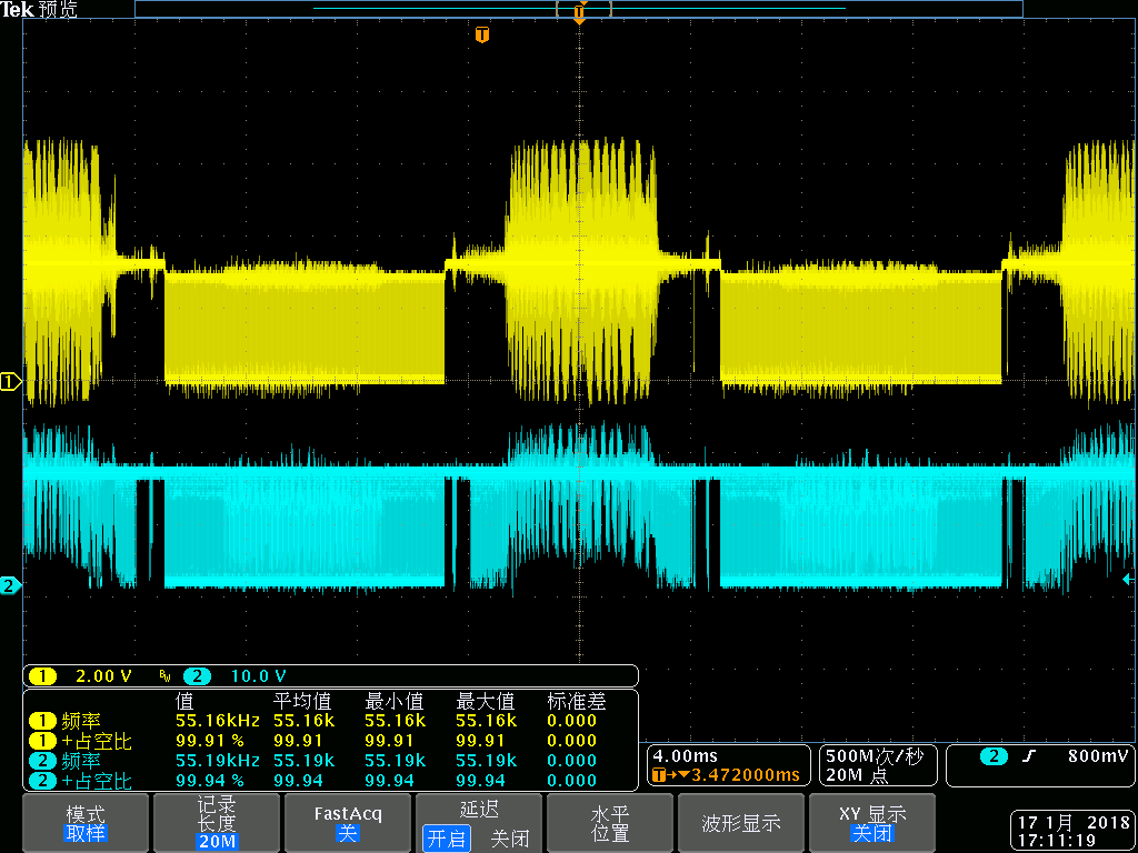
  • They also measured the input and output signal of UCC21520.

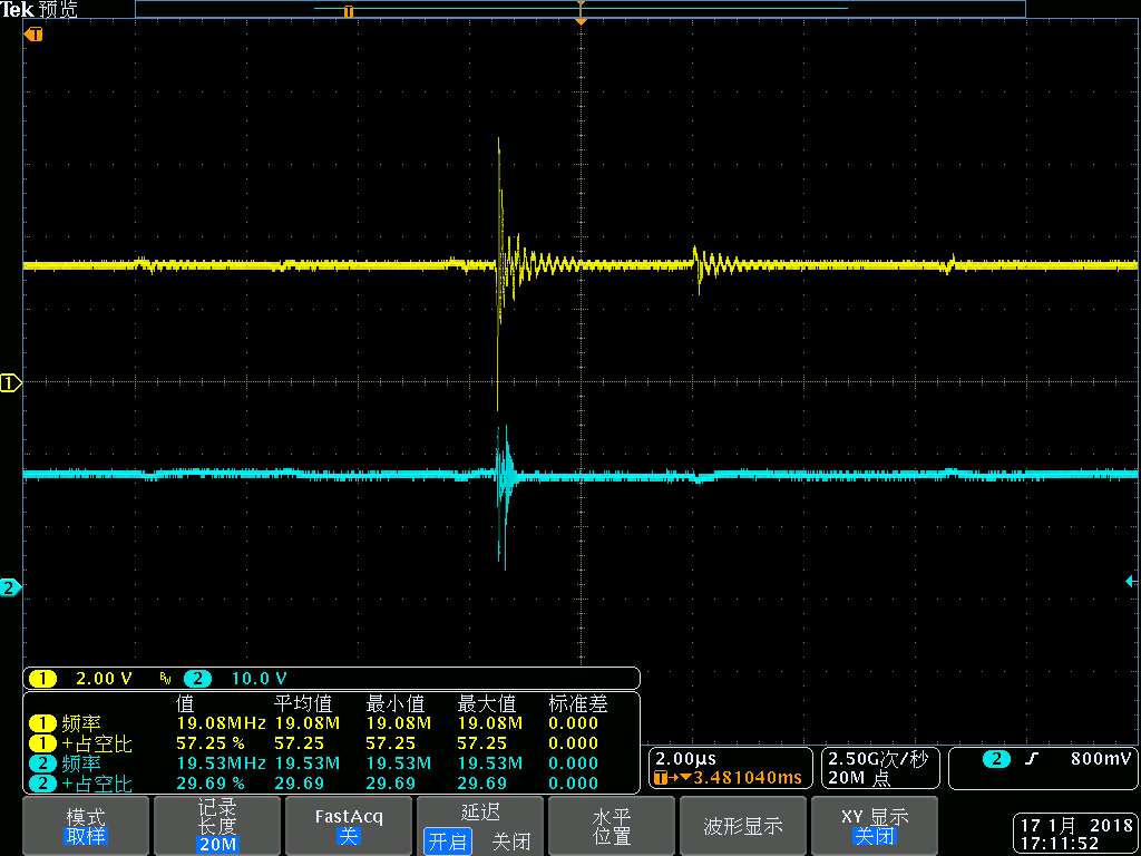
    yellow is input (PWM2d), blue is output (DV2L).

    by zooming in the waveform is like

  • Hello Howard,

    I am an applications engineer with the drivers team. I apologize for the delayed response.

    One possibility is that there is noise on the DT pin causing the DT blanking to activate temporarily. In the datasheet, in the pin description table, the recommended range for the DT pin resistor is between 500Ω to 500kΩ, and a 2.2nF or greater capacitance from DT to GND is also recommended. They could try decreasing the resistor value to within this range and adding the capacitor to DT pin for added noise immunity.

    Another possibility is that this could be noise on the DIS pin. They could try adding a small capacitor (1-10nF) from DIS to GND and see if this helps.

    Another possibility: The noise on the input is very large, exceeding the absolute maximum ratings of the part. Operation outside of the absolute maximum ratings could be causing unexpected output behavior. They could try placing a small (<100pF) capacitor between INx and GND to help filter this noise, and see if this solves the problem.

    These pulses may also be due to exceeding CMTI rating. Do GNDdc and GNDs differ, and if so, what is the slew rate of this difference?

    I will continue to provide support if these suggestions are tested and do not help.

    Regards,