


Other Parts Discussed in Thread: DS32EL0124
My customer have many questions about DS32EL0421 register information in detail.
Would you please advise?
1. Address 02
Q1) Do the pullup/pulldown of bit[7:2] mean internal pullup/pulldown resisters?
Q2) What do “Output Tri-State” and “Output enabled” of bit 0 mean? Open drain or CMOS out?

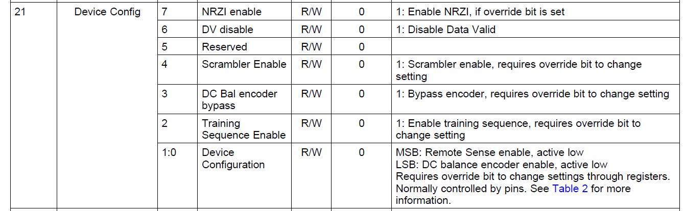
2. Address 21
Q3) What is Training Sequence of bit2?
Q4) What is the difference between disable (DC Bal encoder bypass) of bit3 and enable (DC balance encoder enable) of bit 0?
3. Address 29,2A
Q5) Are "No clock present on TX_CLKIN" and "TxCLKIN not detected " the same meaning?

Your advise would be so appreciated.
Best Regards,
Akihisa Tamazaki

