This thread has been locked.

If you have a related question, please click the "Ask a related question" button in the top right corner. The newly created question will be automatically linked to this question.

TXS0108E: SPI bus high error rate

Part Number: TXS0108E
Other Parts Discussed in Thread: SN74AVC4T774

Hi,

Could you please provide some guidance on how resolve the following issue we are experiencing?

We have a TXS0108E IC to switch logic levels from 1.8V (Qualcomm Snapdragon 410) and 3.3V (STM32F100) and are having issues with many byte errors happening in the SPI communication.

The Qualcomm is the master and the STM is the slave. The SCLK is running at 1MHz (the TXS0108E's datasheet specifies that speeds up to 60Mbps should be doable for push-pull).

The TXS0108E is in the "vicinity" of the Qualcomm processor, and the STM32 is on the "far end". 

We wrote some quick programs to send incrementing numbers out of the Qualcomm and be echoed back by the STM.

The result of this test is: approximately 60% of the bytes came back with errors. When we hooked up the oscilloscope the error rate became significantly larger, over 80% (the probes were set at 10X).

As you can see, transitions look fast but DC levels look bad. There is also some crosstalk and ringing.

Please refer to the following images:
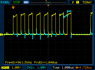
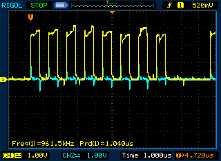
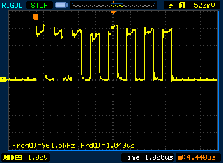
Picture references:

SCLK is yellow

MOSI is blue

The oscilloscope probes were set at 10X

60% byte error rate without the oscilloscope

80% byte error rate with oscilloscope

This diagram shows the interconnection of the devices:

Motherboard
#####################################################
#                SOM + Carrier Board                           "Zeus" board    #
# *******************************************               *****************  #
# * (OPEN-Q 410 SOM) -> TXS0108E * ---------> * STM32F100 * #
# *******************************************  (20cm)  *****************  #
#               1.8V                   1.8V/3.3V                            3.3V          #
#####################################################

The probes were connected on the STM32 side.

The motherboard has SPI routed to 5 expansion slots. The board's SPI routing topology looks like this:

                          Empty Empty Empty
       SOM                |           |         |
Carrier board ---------------------------
                                      |          |
                                 "Zeus"  Empty

The linear trace length on the Moterboard in between the carrier board slot and the "zeus" board's slot is around 20cm. Thace width is around mostly 10 mils (8 mils when fanning out/into board to board connectors) and SCLK, MOSI and MISO rung alongside and are generally space 2x trace widths appart (where possible). The board to board connectors are 90 pin ones out of Hirose's DF40 series. The motherboard is a standard FR4, two layers, 1.6mm thick, 1Oz copper board.

Could you please advice?

Thank you!

Regards,

Alessandro

  • Hey Alessandro,
    I accidentally clicked the "TI thinks resolved" button on your post - sorry about that.

    Thanks for the detailed post. I will ask our translation expert to take a look, but he probably won't get to it until we're back in the office on Monday. Have a good weekend!
  • Hi Alessandro,

    Thanks for your post and the detailed explanation.

    TXS supports 60Mbps push-pull interface, however, it is also under limitations of the output loading.
    Output loading could be in the form of parasitic capacitive loading, output current loading required by the receiver device (STM in this case).
    When you start to probe the IO ports of the TXS, it introduces additional probe capacitance which is indicated by the error rate increase, as you have mentioned.
    Especially if there is a fan out of the SPI signals into different slots, I would not use this TXS0108 device which provides no more than 20uA of DC drive through its  internal pull-up resistors.
    I would instead suggest using the SN74AVC4T774 which has individual DIR control pins to control the signal flow and suit it for SPI interface. It also provides enough DC drive 12mA per channel to fan out the signals to all the expansion slots as well.

  • Hi Shreyas,

    Thank you for your answer. However, the IO pins on the Qualcomm are multiplexed so it's very hard to know beforehand the direction each pin should have. In our current approach we are doing the logic level translation before the de-muxing, to minimize the amount of logic level shifting ICs. The de-muxing is currently being handled by analog switches.

    Does TI offer a similar logic level translator IC that offers high DC drive strength? Or are there bi-direction level translators that also handle muxing/demuxing?

    Regards,

  • Alessandro,

    The high DC drive strength translators are direction controlled like the one I pointed out earlier SN74AVC4T774.
    Limiting the DC drive strength is critical to achieving the auto bidirectional feature like TXS or TXB device.
    I know that there are switching Mux which could do down translation but not which can handle up translation.
  • Hi Shreyas,

    Ok, I appreciate your answer. For the time being I'll try lowering the SPI speed in the hope that the capacitive effects will be less noticeable.

    Thanks!

    Regards,

  • Thanks Alessandro.
    I will be curious to know the results of it.
    If there is a way to reduce the overall distance that should help to significantly reduce the capacitance as well.