

We have noticed a behavior in several of our devices that we cannot explain 100%.
We have a serial data link with four signals routed via two ISO7420ED.
Both isolators are supplied by the same voltage. They are directly next to each other in the layout, and are connected to the supply planes in the same way. So they both have the same supply voltage levels.
With power-down on the input side, dynamic signals (clock and a control signal) are present at the signal inputs of one of the two isolators. On the second isolator, the two signal inputs are static (low).
This ISO7420ED with the static input signals obviously goes into fail-safe state earlier than the one with the input signals that change their level continuously.
We have seen in the data sheet that also inputs with undefined levels at the ISO7420ED can lead to the fail-safe state at the outputs: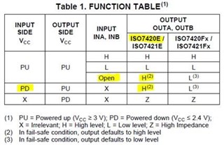
However, we were able to exclude this after our measurements.
Does the signal shape - static or clocked - at the signal inputs (INA, INB) of the ISO7420ED have an influence on the fail-safe behavior of the signal outputs (OUTA, OUTB) in case of input-side (INPUT SIDE Vcc) power-down?
Regards Bernd

-
Ask a related question
What is a related question?A related question is a question created from another question. When the related question is created, it will be automatically linked to the original question.

