This thread has been locked.

If you have a related question, please click the "Ask a related question" button in the top right corner. The newly created question will be automatically linked to this question.

ISOW1432: Noise in voltage rail

Part Number: ISOW1432
Other Parts Discussed in Thread: ISOW7841

Hi,

We are facing noise issues in the VDD pin, VISOOUT, and Vio pin. ( measured values are-> 124mv,200mv,101mv,),

Vio pin connected to 1.8v regulator that output noise 40mv only. 

I'd like you to review my schematic. The schematic  I will send the privet message.

Sincerely.

  • Hi Anoop,

    Thanks for reaching out. 
    Could you please confirm that I can reach out to you over your email ID which you have used for creating your TI account?

    Regards,

    Koteshwar Rao

  • Hi Koteshwar Rao,

    Thanks for repaying,

    I send a friend request in TI. Please accept.

  • Hi Aoop,

    Thanks, I have accepted the friend request. I will look forward to the schematic, thanks.


    Regards,
    Koteshwar Rao

  • Hi Koteshwar Rao ,

    Any updation

  • Hi Anoop,

    Thanks for sharing the schematic.

    I have reviewed the schematic and it mostly looks good, I didn't see anything major to worry about. Just one suggestion regarding the ferrite beads. I see that you are currently using a 0Ω resistor R1711 between device GND2 pin and AISG_GND. It is recommended to use the same ferrite bead on both VISOOUT and GND2 line to filter out the noise, especially common-mode noise. This might or might not change the noise that you are observing but otherwise is a general guideline that we would like you to follow to get the optimum performance from ISOW1432.

    The same applies to VDD and GND1 pins but it isn't as important as VISOOUT / GND2.

    Higher noise on supply pins can happen if the decoupling capacitors aren't close to device pins as recommended in the datasheet. I would like to review the PCB layout to see if there are any concerns in PCB layout that are leading to high supply noise. Could you please share the PCB layout?

    Please do also share the waveform of noise that you have observed on VDD, VISOOUT and VIO. I would like to know what kind of noise you are observing on these pins and their frequency. Thanks.


    Regards,
    Koteshwar Rao

  • hi, Koteshwar Rao,

    Please check the private message

  • Hi Anoop,

    Thanks for sharing the waveform.

    I see that the waveform shows random voltage spikes which occur in random order and do not have a fixed frequencies. It doesn't look like these are generated by the ISOW1432 and they seem to be noise picked up the oscilloscope probe. Any switching noise from ISOW1432 would be repetitive with a frequency and same amplitude all through.

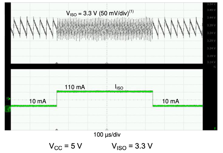
    Please refer to an example output ripple waveform from another device (ISOW7841) for reference. This is a noise contributed by device and it is repetitive and has a fixed frequency for given load condition.

    Please do try to test with a different oscilloscope probe or in a different environment to bring down the noise from external sources. Please also make sure the ground connection from the probe is connected to device GND closest to device pin to get the most accurate error free waveform. Let me know if you have any questions, thanks.


    Regards,
    Koteshwar Rao