This thread has been locked.

If you have a related question, please click the "Ask a related question" button in the top right corner. The newly created question will be automatically linked to this question.

SN6505A-Q1: Minimum specification of 'output switch voltage'

Part Number: SN6505A-Q1
Other Parts Discussed in Thread: SN6501, SN6505A

Hello Team, customer needs following information:

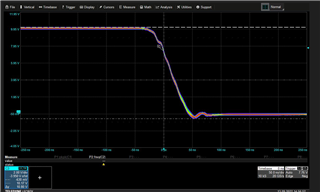
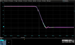
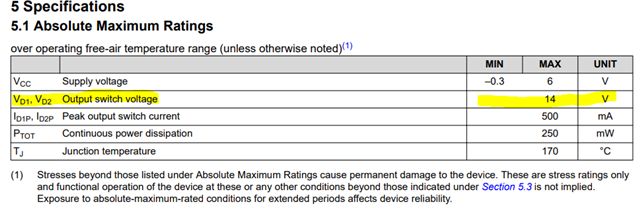
Is there a minimum voltage value for D1&D2 specified? For example negative values.

Especially maximum continous DC or peak AC for negative voltages.
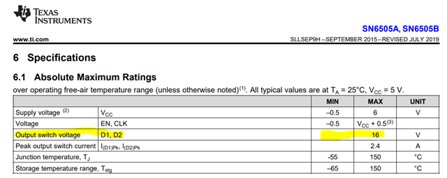
And same for SN6501

Many Thanks

Josef

  • Hi Josef,

    Thanks for reaching out.

    The D1/D2 pins do not support negative voltages, hence, you can read the minimum voltage as 0V. Since MOSFETs of SN650x on D1/D2 pins are on the low-side, we do not expect to see negative voltages and hence, this shouldn't be a concern. Let me know if you have any further questions, thanks.


    Regards,
    Koteshwar Rao

  • Hello Koteshwar,

    Thanks for the reply. I have done few measurements on my PCB:

    D1:


    D2:


    I measure here the maximum negative peak of -630mV. Then would it be a problem?

    Regards,
    Nisarg Mehta

  • Hi Nisarg,

    Thanks for reaching out and for sharing the waveform.

    The MOSFETs on D1 and D2 pins inside SN6505A have their body diodes that will get forward biased for negative voltages. Hence, most negative transients should get clamped to voltages between 0.7V to 1V. Hence, seeing -630mV is expected and shouldn't be a problem. Thanks.


    Regards,
    Koteshwar Rao