A related question is a question created from another question. When the related question is created, it will be automatically linked to the original question.
If you have a related question, please click the "Ask a related question" button in the top right corner. The newly created question will be automatically linked to this question.
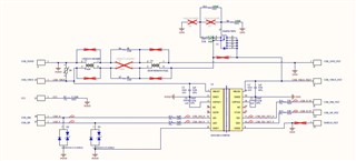
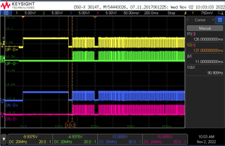
during system power up the downstream port D+/- signals do not match the upstream port. Attached are the schematic and a scope shot of what is being seen. What is the cause and what can be done to fix it?
For additional context about the observed behavior, the issue is seen when the USB-C cable is plugged into various USB power adapters. D- being held low is forcing the device to enter USB Suspend mode and not be properly powered up.
Thanks for reaching out and for sharing the waveform and schematic.
I see that the signals on upstream side of ISOUSB are really slow, not sure if this is an expected behavior for such inputs. Please allow me to check with the experts on this topic and come back to you.
In the meantime, I see the power supply is being passed from the left side to the right while the GNDs are separated. I am not sure if this will power VBUS2 as GND2 is floating with respect to supply on VBUS1. Could you please confirm if VBUS2 / GND2 was supplied with an external supply while testing? If not, could you please short both supplies and both GNDs for testing purpose and let us know the results?
Koteshwar, VBUS1 is powered from the input cable. VBUS2 is powered by the same source but after it goes though the common mode chokes and the inrush current limiter. Due to the Common mode chokes yes the grounds are also isolated. The circuit works when connected to a USB hub but not when connected to USB A or a USB wall adapter
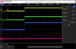
Koteshwar, your requested images with the supplies shorted. In summary HUB and the USB on the power supply work but USB A and USB C wall adapters do not.
USB HUB connected to computer with VBUS1 and VBUS2 shorted together
USB port on a power supply with VBUS1 and VBUS2 shorted together
USB A wall adapter with VBUS1 and VBUS2 shorted together
USB C wall adapter with VBUS1 and VBUS2 shorted together
For reference the full part number is ISOUSB111DWXR (SSOP)
A couple of related questions came up today
1. Is the die the same between the two packages DWR and DWXR
2. pin 12 on the DWR package is labeled PIN and recommended to pull up to 3.3V. Pin 12 on the DWXR package is V1OK. Is PIN internally pulled up in this package?
3. What are the functions of Pins 4 and 13? currently left floating but should we pull up to 3.3V?
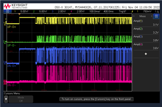
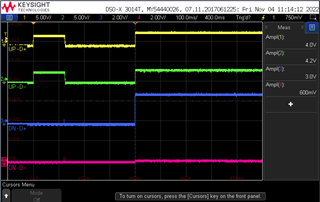
As built this is how the signals look when connected to a USBhub
Thank you for sharing additional information and waveforms, this is helpful.
To make sure I understood the issue correctly, please allow me to rephrase the issue below based on my understanding.
ISOUSB111 is used in your product which is a device and not a host. Your product is a self-powered USB device.
When your product is connected to a hub that connects to a computer or connected to a computer directly, your product is working fine and the UDx and DDx lines of ISOUSB in your product are matching.
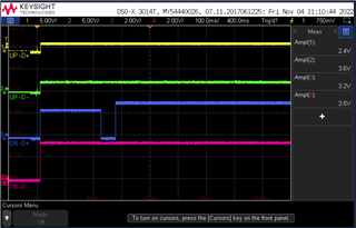
But when your product is connected to a wall adapter (Type A or Type C), your product doesn't work and UDx and DDx pins of ISOUSB do not match.
Please correct me if my understanding is not accurate.
Assuming my understanding is correct, I have the following questions.
When your product is connected to a hub or a computer, I believe you are sending information from the computer to your product and verifying the data on UDx and DDx pins of ISOUSB.
When your product is connected to a wall adapter, how are you sending data on UDx of ISOUSB?
Since the USB port from your product is connected to a wall adapter, I believe there is no provision to send data to your product unless you have tapped the UDx pins of ISOUSB using wires and connected them to another hub or computer.
I am assuming that your product is not expected to receive any data when it is connected to a wall adapter. If it is a battery powered device, then it should only charge during this time.
Or did you mean to only ask why the waveforms on UDx and DDx not matching even when your product is connected to a wall adapter?
In the above waveform, it looks like the adapter is pushing an SE1 on UDx pins, i.e., a single-ended '1' on both UD+ and UD-. This is an invalid input and the device doesn't reproduce the same at DDx pins. Instead, I believe it is sending out a J-state pushing the USB device to idle state, like you already pointed. This seems to be an expected behavior.
It maybe that the adapter is build to do this intentionally so that the device goes to idle state during charging. Hence, there is no data transactions on the USB which I believe is an expected use-case with a wall charger. If my assumptions or understanding is incorrect, please do help clarify the application, the use-case, expected behavior and any other information you can. The more I know about the application and use-case, the quicker we will be able to identify the cause and resolve it.
Please allow me to address the questions you have listed out in your last post.
2. pin 12 on the DWR package is labeled PIN and recommended to pull up to 3.3V. Pin 12 on the DWXR package is V1OK. Is PIN internally pulled up in this package?
Yes, PIN is internally pulled-up to V3P3V2 for the DWX package.
ISOUSB111 is used in your product which is a device and not a host. Your product is a self-powered USB device. Our system is a bus powered device
When your product is connected to a hub that connects to a computer or connected to a computer directly, your product is working fine and the UDx and DDx lines of ISOUSB in your product are matching. Correct
But when your product is connected to a wall adapter (Type A or Type C), your product doesn't work and UDx and DDx pins of ISOUSB do not match. - Mostly correct. When connected to a wall adapter the UD+ (logic 1) and DD+ (logic 1) match. However, the UD- (logic 1) and DD- (logic 0) do NOT match.
Please correct me if my understanding is not accurate.
When your product is connected to a hub or a computer, I believe you are sending information from the computer to your product and verifying the data on UDx and DDx pins of ISOUSB. - UDx/DDx data validation is assumed based on USB enumeration and normal USB bus activity. In other words, the product enumerates and stays enumerated while connected to a computer.
When your product is connected to a wall adapter, how are you sending data on UDx of ISOUSB? - UDx "data" is generated by the wall adapter. Based on the scope captures, it appears that the wall adapters are outputting static logic 1's on both D+ and D-.
Since the USB port from your product is connected to a wall adapter, I believe there is no provision to send data to your product unless you have tapped the UDx pins ofISOUSBusing wires and connected them to another hub or computer.- Correct. We can NOT send USB data when connected to a wall adapter.
I am assuming that your product is not expected to receive any data when it is connected to a wall adapter. If it is a battery powered device, then it should only charge during this time. - Correct. However, this USB powered product needs to know whether it is connected to a wall charger (D+ = D- = logic 1) or a computer. This is required to support disabling the product when the host enters USB suspend, e.g. laptop in suspend. Currently, the method for the product to enter sleep mode is to monitor the D+ / D- lines for lack of USB activity [D+ = 1, D- = 0 for >Xms]. Since USB chargers have D+ and D- both set to 1, the system should not enter suspend mode.
Or did you mean to only ask why the waveforms on UDx and DDx not matching even when your product is connected to a wall adapter? - That is the question. Why does UD+ (1) == DD+ (1), but UD- (1) != DD- (0)? Additionally, is there anything that we can do from the downstream device to cause the ISOUSB111 to accurately reflect the state of the UDx pins when there is no USB activity? For example, a forced SE0 event from the downstream device?
The output of the schematic is attached to a processor in a charging stand. It senses USB activity to turn on the wireless charger in the stand.
Thank you very much for your detailed inputs, appreciate it.
I am checking with the team internally to find out the reason why both DDx pins are not becoming a logic '1' to reflect the the inputs at UDx pins. I am also checking to see if there is anyway to make the outputs go logic '1' in this test condition. I will keep you posted on this, thanks.
We have had offline discussion further on this issue and we confirmed that ISOUSB111 does not reproduce SE1 (invalid input) that is appearing on its upstream side onto the downstream side. We have also suggested that use of a USB charger detection device, like BQ24392, is recommended to make sure various types of USB chargers are detected correctly.
Hence, I will go ahead and mark this post as closed. If you do see any further questions, please feel free to respond to this post or create a new one, thanks.