This thread has been locked.

If you have a related question, please click the "Ask a related question" button in the top right corner. The newly created question will be automatically linked to this question.

LM5180: DATASHEET

Part Number: LM5180
Other Parts Discussed in Thread: LM5185, LM25180

Tool/software:

Hello, TI team

I am studying LM5180/LM5185 for MOSFET gate drive PSU and have some questions troubling me.

Appreciate you could help to clarify it.

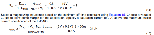
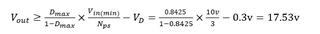
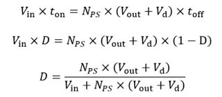
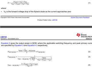
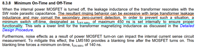
1. The Min magnetizing inductance calculation is descripted at page19 of LM5180 datasheet as below.

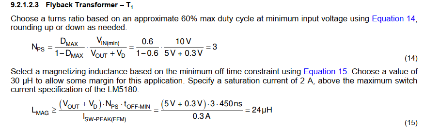
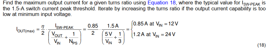
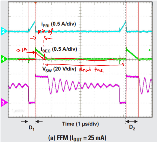
If Toff-min=450ns is used for calculation, the related duty cycle D≥1-Fsw*Toff-min=1-450ns*350khz=84.25%, but the Dmax set at 60% in BCM operation mode, how to understand equation 15 and how to get equation 18?

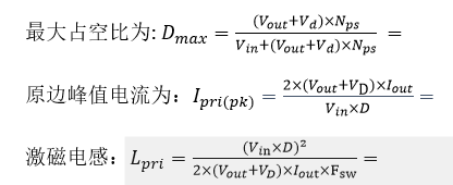
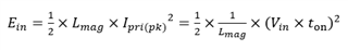
TBH, the related description for magnetizing inductance calculation in LM5185 datasheet is easier to understand.

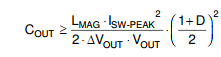
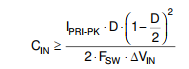
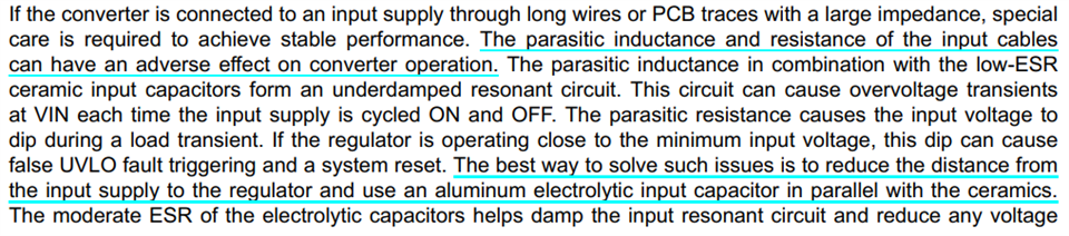
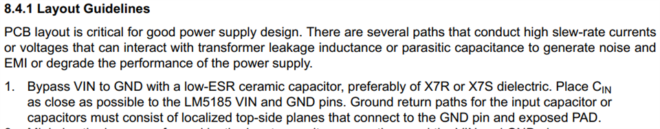
2.Regarding Cin, the related description at page 22 of LM5185 datasheet as below. but recommend low-ESR ceramic capacitor regarding Layout Guidelines, which is better? and same recommend capacitors are descripted in LM5185 EVM

Best regards

Hailong

  • Hi Hailong,

    Thank you for posting.  These are good questions, and they are related to the tradeoff decisions in design. 

    Regarding your 1st question, 60% max duty is an empirical choice. Yes you can set Dmax=85%, but you would end up with bigger Pn : Sec transformer turns ratio, and hence the higher voltage stress SW pin.  In addition, the time to transfer the energy to the load is reduced to a verry narrow time window, which mean high rms current on the secondary winding and hence the winding conduction losses.  Thirdly, you would need bigger Cout to achieve your Vout ripple spec. 

    Regarding your 2nd question,  you need a combination of ceramic and electrolytic.  The ceramic capacitors filters the ripple current, and the electrolytic for damping of the resonant tank formed by the inductance and the ceramic capacitors.  Please read the following article for details.

    https://www.ti.com/lit/pdf/snva538?keyMatch=input%20filter&tisearch=universal_search

    Hope this clarifies. 

    Regards,

    Youhao

  • Hello, Youhao,

    Thanks a lot for your kindly support.

    Sorry, I didn't descript the question clear.

    Regarding 1st question, I couldn't understand equation 15, where Nps=3(based on D= 60% ),Toff-min=450ns(calculate D≥84.25%),please see following snapshot.

    My understanding is magnetizing inductance calculation is based on following equation step by step, Toff-min is only a limit value to double check duty cycle(toff=(1-D)/fsw) but couldn't be used to calculate magnetizing inductance. Please correct me if I am wrong.

    Regarding 2nd question, thanks a lot for sharing reference document, it solved.

    Question 3, TBH, I like to derive the formulas to understand them better, could you share some proposal to study equation 18, equation 22, equation 24.

    Question 4, I am preparing isolated PSU for MOSFET drive, input voltage range is from 8v to 20v, output 20v&0.15A, do you have any recommended DC/DC converter regarding the design?

    Best regards 

    Hailong

  • Hi Hailong,

    Equation (15) is regarding the secondary circuit:  the secondary current pulse duration should  be >450ns. This is the min duration for proper operation. Note that the IC sense the output voltage at the end of the secondary winding current. Namely at the moment when the secondary current drops zero.  To have accurate sensing and hence good Vout regulation, the IC takes time to prepare itself for the sensing moment. The max time to get ready to Vout sense is 450ns.  That means, the secondary current should flow not shorter than 450ns.  

    When the secondary flows, the current decays linearly from the peak current.  The shortest time duration is related to the min peak current, and the min peak current is Ipk_FFM, which is 0.3A on the primary side, and translates to be 0.3A *Nps on the secondary side. 

    And, the secondary inductance is Lmag * Nps^2.  Doing the inductor current duration V/L * 450ns, you will get equation (15).  

    Regarding your question 3, I will need some more time about the Cout and Cin equations.  For Iout(Max), it is determined by the primary IC peak current.  Translate it to the secondary, the secondary pk would be Ipkmax * Nps.  It is another triangle, and the BCM time duration for the secondary circuit is (1-D)  you can get the average input current. 

    Iin = Isw_pk* 0.5 * D

    Duty= Vout / (Vout + Vin / Nps)

    Pin = Iin * Vin

    Po = Pin * Eff

    Work from these you will get equation 18.

    Please wait until next week for how to get the other two equations. I am also suggesting you to find a power electronics text book to get more insight about the basic calculations of flyback converter parameters. 

    Regarding your question 4. the LM25180 should be a good fit. Please use our design calculator to help you design.

    Thanks,

    Youhao

  • Hello, Youhao,

    Thanks a lot for your kindly support.

    Regarding question 1, let me put it another way.

    Due to Nps=3 is a factor in equation (15), it means Dmax=0.6 is fixed, see equation (14).

    Toff(min)= 450ns is another factor in equation (15),so, fsw>(1-d)/Toff(min) = (1-0.6)/450ns≈889Khz, but the max switching frequency is 350Khz。

    even if the duty cycle increases to D=84.25 at max switching frequency 350Khz, see following calculation, but target Vout=5v

    Based on following calculation, Ton should be very low in FFM mode, means Duty cycle decrease to reduce energy.

    So, It is not meaningful to calculate magnetizing inductance with equation (15). Please correct me if I am wrong.

    Regarding question 3, 

    Compared with your calculation,  Vd is ignored.

    Vd appears in above other equations, sudden disappear and no any notice, it makes me doubt my calculations.

    I know some factors are ignored for approximate calculations, such as Vds(on), Vr(sen), and they are too low compared with Vin never appear in the datasheet.

    As you know, approximate calculation and WSC have different impact on components.

    Best regards

    Hailong

  • Hi Hailong, 

    Sorry I think you have a wrong concept or understanding about the operating principle of this PSR flyback.  What you derived is based on a regular fixed frequency flyback theory.  At 350kHz, the off time is no longer 450ns.  

    My colleague published an article, in which he detailed the three different modes:  BCM, DCM and FFM.  Hopefully this can help clarify your questions.

    https://www.ti.com/lit/pdf/slyt779?keyMatch=PSR%20flyback&tisearch=universal_search

    Thanks,

    Youhao

  • Hello, Youhao,

    Sorry, I still couldn't get your point.

    The description you shared is below, and the max frequency is 350Khz, if Toff =45ns, could you point out the related frequency, duty and Toff?

    Compared LM5180(with build-in MOSFET) datasheet and LM5185(without build-in MOSFET)  datasheet, similer datasheet and application, but different magnetizing inductance calculation equation. 

    The snapshort is from LM5185, same as my wrong concept or understanding.

    Best regards

    Hailong

  • Hello Hailong,

    Engineer supporting this thread is out of office and will be back to answer your thread tomorrow, thanks for your patience.

    David.

  • Hi Hailong,

    Let me try in a different way. 

    First, the 450ns is the required duration, (yes, the required for normal operation), for the secondary current to flow.  In other words, the secondar current must flow at least 450ns. This is also called the min off-time, because the secondary current flows after the main switch is turned off.  

    This is why the secondary inductance must satisfy that:  Isec_peak = (Vo+VF)/Lsec *450ns.  Namely the current must last longer than 450ns.

    Since Lsec = Lmag / Nps^2,  and Isec_peak = 0.3A for the LM5180, put these into the equations, you will get equation (15). 

    If you select a bigger inductance, this min off time in your circuit will be greater in accordance. 

    I think the word "off-time" may cause confusion to you. We may need to change it to "the secondary current conducting time", because in DCM (350kHz switching), after the main switch is off, the secondary side conducts for some time, the rest of the cycle is "dead time" during which both the primary FET and secondary diodes do not conduct.  See below if the Lmag is just choose by 450ns min-off time and you operate the circuit at the boundary of FFM and DCM.  Then the switching frequency is 350kHz, the on time, the secondary conducting time and the dead time all makes up for ~2.86 us. During DCM, the deadtime is changing with the on time, and secondary conduction time, to make the cycle remain in 2.86us.

    Hope this helps.

    Best Regards,

    Youhao

  • Hello,Youhao

    Thanks a lot for your kindly support.

    Yes, you are right. I confused the "off-time" with "higher part of dead time" from below description.

    Due to the dead time is long enough in FFM, and trough voltage induction. Even if the toff time exceeds 450ns, it shouldn't have any impact on the secondary zero-current detection.

    Please help to clarify another question.

    As mentioned, LM5180(with build-in MOSFET,0.3A) and LM5185(without build-in MOSFET,20mv) are similar converter, but different calculation, how to understand?

    LM5180 datasheet: magnetizing inductance is calculated in FFM.

    LM5185 datasheet: magnetizing inductance is calculated in BCM.

    Best regards 

    Hailong.

  • Hi Hailong,

    First, the LM5180 has fixed current limit which you can not change it, but you can directly refer to the current value.  The LM5185 has adjustable current limit which you can change by changing the Rcs resistor value. The Rcs converts the current to a voltage for the IC to use, so we refer to 100mV and 20mV for the max and min peak current limit thresholds. You can change Rcs value to adjust the actual current limits. 

    Regarding the 450ns off time, it is required by the IC for proper operation.  Your off time can be short, but the Vout sense would not be accurate because the Vout sensing point should be at least 450ns later following the primary switch turn-off moment.  The internal circuit takes time to be ready for Vout sensing.  If your zero cross comes early, when the Vout sensing moment comes, the winding voltage is no longer at the zero crossing moment, and your Vout regulation will become inaccurate.

    Regarding the Lmag calculation, there are different design philosophies.  The LM5180 watches the 450ns requirement to get a min required Lmag, and the LM5180 targets the possible optimal operation frequency under the nominal input voltage, for which would the most time the IC will operate under.  In addition, it also needs to check against the 400~450ns required min off time.

    Hope this clarifies.

    Best Regards,

    Youhao