


Hi
I am trying to understand the effect, if any, of a common mode RF sinusoid applied to the receiver inputs. It seems that the relevant parameter to look at is the -9V to 14V max pin voltage listed in table 7.1. Is that a static parameter (i.e. damage will occur if >14V is applied to the pin indefinitely), or is there a time element associated with it? Also, what is the expected failure mode for a voltage on the input pins that exceed the datasheet range (-9V to 14V) for the A/B inputs? For reference, here is the circuit:
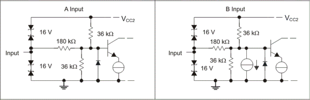
In particular, I'm am curious about the negative limit. If -10V, for example, is put on the Input, I'd expect to see the diode near the base of the BJT to forward bias, but the resistance in that path is quite high, so I wouldn't expect much current to flow (~52uA), and therefore I do not expect the power dissipated in the diode to exceed a few hundred microwatts. So, I doubt that is the failure mode. I think -10V shouldn't be enough to cause the 16V protection circuit to turn-on either...although, I guess the voltage between VCC2 and Input is close to about 16V if VCC2 is at 6V.
Any details you could share would be greatly appreciated. Thanks!
Paul
