This thread has been locked.

If you have a related question, please click the "Ask a related question" button in the top right corner. The newly created question will be automatically linked to this question.

ISO7721: Using ISO7721 instead of optoisolator

Part Number: ISO7721
Other Parts Discussed in Thread: ISO7720, ISO7710,

Hi,

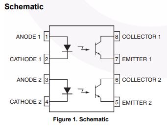
I'm currently using optoisolator(MOCD207M) for charge enable of my design. 

PIN1- ANODE 1: 3.3V

+470ohm serial resistor

PIN2-GND_A

PIN8-COLLECTOR 1: Pin of IC

PIN9-EMITTER 1: GND_B

The pin of IC goes to LOW for charge enable.

If it is possible, I would like to use ISO7721 instead of optoisolator.


Is there any problem for my application? 

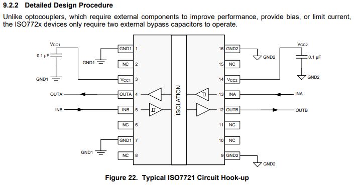
By the way, why OUTPUT_A located on the left side but OUTPUT_B located on the right side? I think it is problem for PCB layout.

Thank you.

  • Hi Nedd,

    Thank you for using E2E forum.
    It should be perfectly fine to use ISO7721 for your application if you need two isolation channels with one in each direction. If you need two channels to be on the same direction like it is in the Opto part that you have shared in your post then you can use ISO7720. The ISO77xx family has devices in 1, 2, 3, 4 & 6-channel configuration and available in various package options. Please choose the one that suits your application the best.

    I understand your concern for channel A being in right-to-left direction while channel B is in left-to-right direction. One of primary reasons for us to choose such a channel direction configuration is that there were already existing competition parts that had followed this channel direction option. Hence to make it convenient for customers to use TI parts, we went ahead with the same channel direction configuration as existing competition devices. I hope this answers your question, thanks.


    Regards,
    Koteshwar Rao
  • Dear Koteshwar Rao,

    Thank you for your rapidly response.

    1)There are basic circuit right now witch optocoupler as I said. 3.3V supply to ANODE 1 and ANODE 2 (with 470ohm serial resistors for 7mA). 

    The pin of the IC-1 is in COLLECTOR-1. The pin of the IC-2 is in COLLECTOR-2. (grounds seperately) 

    When we want to bring the pin of the ICs to ground (this meaning charge enable), we supply a 3.3V supply voltage to ANODE-1 and ANODE-2 together.

    Can I make this switch with ISO7720?

    2) Should I use ISO7720 or ISO7720F for this switching? Which one is better? Is there any reference design like optocoupler.

    3) Should I use 2 isolated supply for  Vcc1 and Vcc2 ? But I have to use only 1 supply(3.3V) for that. Is it possible?

    4) Do you have any other recommend for this application?

    By the way, If it is possible I would like to send my schematic(isolation part with optocoupler) by e-mail for checking.

    Thank you.

  • Dear Nedd,

    Please find below my inputs.

    1) Yes, you can achieve the same optocoupler function with ISO7720 as well and with ease. The internal construction of ISO7720 is very different from an optocoupler but usage of input/output channels is exactly like any other CMOS digital I/Os (like in MCU, MPU, logic devices, etc). When the input to ISO7720 (like INA) is LOW (< 0.3*VCC1), the corresponding output (OUTA) will be pulled to GND. When the input is HIGH (> 0.7*VCC1), the output will be pulled to VCC2 through internal series resistor.
    In ISO7720, OUTA & OUTB share the same GND (GND2) and so is the case for INA & INB sharing same GND (GND1). Hence, the outputs OUTA/OUTB will be referenced to same GND and can't be separated. If your applications needs the two outputs to be connected to two separate GNDs then you will have to use two ISO7710 devices that can be operated independently.

    2) ISO7720 & ISO7720F only differ by the default state output. This means that when input is not powered or left floating, the corresponding output goes to a default state. This state is HIGH for ISO7720 and LOW for ISO7720F. You can use either of them based on what default state you prefer for your application. Functionally, you shouldn't see any difference when you use either of the devices.

    3) VCC1 & VCC2 are on two ends of isolation barrier. To maintain isolation (which is why an isolator is used in the first place), you will have to apply isolated supplies to VCC1 & VCC2. Since the device has two independent sets of circuit one powered by VCC1 and the other by VCC2, the device will be functional even when you use the same supply for both pins.

    4) You can use ISO7721DEVM for your reference and evaluation.

    Yes, you can send me the schematic for review through e-mail. Can I go ahead and write to your email that you have used to create your profile on E2E?


    Regards,
    Koteshwar Rao
  • Dear Koteshwar Rao,

    Thank you.

    Okey, I'm waiting your e-mail.