This thread has been locked.

If you have a related question, please click the "Ask a related question" button in the top right corner. The newly created question will be automatically linked to this question.

ISO7331FC: VCC1 and VCC2 power

Part Number: ISO7331FC
Other Parts Discussed in Thread: LM5035,

Hi Team,

my customer has the following question. Could you please help us here.

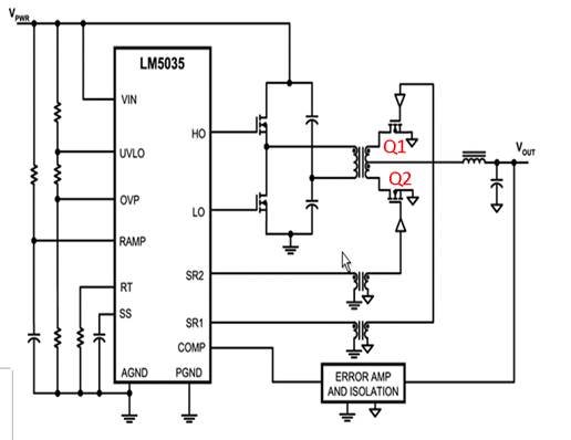
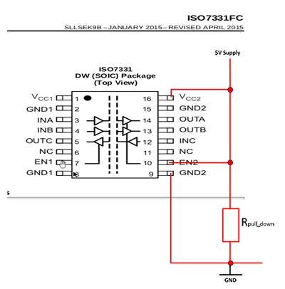
I have a technical question to a digital Isolator ISO7331F. Unfortunately the datasheet was not able to answer me this question. I use this Part for the synchronous Rectification Signals  (SR1 and SR2) on the secondary side of a Power Supply Modul, which I realize with the TI Product LM5035.In my Application VCC1 is always Powered Up first and then VCC2. The SR1 and SR2 Signals will be transferred via INA and INB to OUT A and OUT B and then to a driver to switch on and off the MOSFETS Q1 and Q2. It is very important, that the Signals OUT A and OUT B must have a low Signal when VCC2 is not Powered at the beginning or fails. The may not have a HIGH Signal at the same time, otherwise I would have a short circuit. In the datasheet I just read UNDETERMINED. Does that mean, that they could have LOW OR HIGH or are the outputs TRI_STATE and I can Pull down OUT A and OUT B? Can I put them to a defined low Signal, by Pulling down the EN2, and after VCC2 is Powered EN2 has also a high Signal and the OUT A and OUT B are same as IN A and IN B. (See Figure 1 and 2 below)


Fig: 1

Fig 2:

The question is: Can I put OUT A and OUT B to a defined State (Low, in order to avoid short Circuit) when VCC2 is not available or is  that not possible ?. Do you have an idea, if I can realize that with the ISO7331F or can you suggest another part?


Thank you in advance.

Best Regards,

Needhu

  • Hi Needhu,

    Thanks for reaching out to us with the customer question.

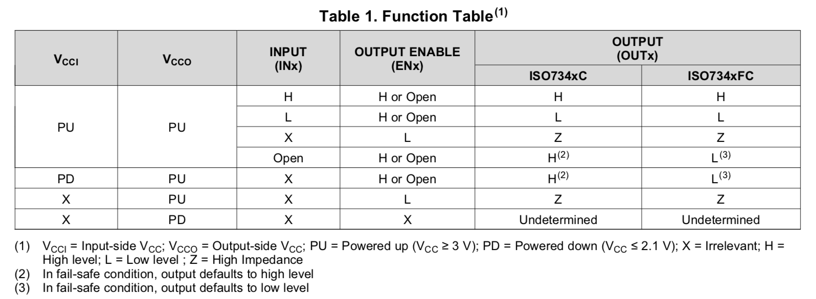
    You are correct in saying that the function table provided in ISO7331FC datasheet states that OUT pin state is undetermined when its respective VCC is in power down (PD, VCC<2.1V) [as also shown below]. The reason we state it as undetermined is because under this condition the device is not powered-up but there is still some insufficient voltage at VCC. This can partially power-up some components and some of this voltage may or may not the output. In most cases, we expect the output to be close to 0V but this cannot be guaranteed as the device is not powered-up to fully control the output. Even if you see some voltage at OUT pin under these conditions it would be much lower than 2.1V.

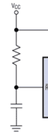
    Having said that, we do recommend having a pull-down resistor (about 4.7kΩ) at OUT pin to make sure any residual charge is drained out to GND. In addition, customer can also think of using an RC delay circuit at EN pin (as shown below) which holds EN pin at LOW until device is completely powered-up. When EN pin is LOW output is clearly going to be tri-stated and the pull-down resistor at OUT pin will make sure the output is read as LOW.

    The value of RC can be chosen such that the delay is sufficient enough for the device to fully power-up.

    I would also like to recommend using ISO7731F over ISO7331FC as the ISO77xx is our latest digital isolator family offering the most robust performance. It is also useful for this situation as ISO77xx has PD at 1.7V as against ISO73xx which has this at 2.1V. This means that ISO77xx can power-up at lower voltages than ISO73xx can.

    Let me know if you have any questions, thank you.

    Regards,
    Koteshwar Rao