This thread has been locked.

If you have a related question, please click the "Ask a related question" button in the top right corner. The newly created question will be automatically linked to this question.

ISO5452: High Side driver

Part Number: ISO5452

Hi

Our customer going to use this device as a high side driver.( e.g. high side driver of half bridge topology)

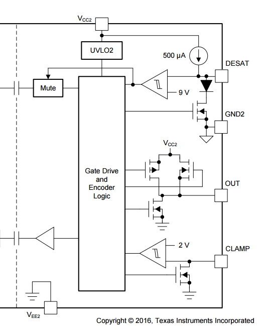
How can we connect the GND2 of ISO5452? Should we connect GND2 to SW(switching) node? or GND node of secondary?

I refereed the following document for using low side driver as high side driver. 

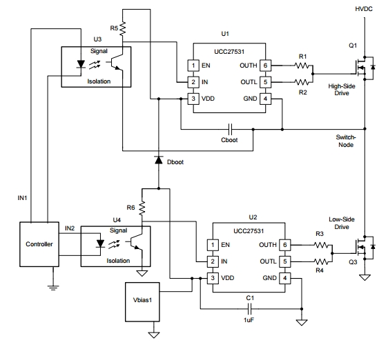
http://www.ti.com/lit/an/slua669/slua669.pdf

If this connection is not match to this case, please advice to me how can we connect the GND pin.

Regards,

Koji Hamamoto


  • Hi Koji Hamamoto,

    The above circuit presented is correct. Even in case of isolated gate driver,  GND2 of the high side gate dirver is connected to emitter of the high side switch as shown in the figure below

    Please let us know if you have further query 

    Regards

    Tejas

  • Hi Tejas,

    Thank you for your prompt reply.

    As the following block diagram is shown, 


      >> GND2 can be connected to the emitter of high side switch.

      >> VEE2 is connected to the GND of secondary side.

    Is my understanding correct? 

    My concern is that the GND2 moves according to switching if it is connected to emitter of high side switch. Is that ok?

    Regards,

    Koji Hamamoto

  • Hi Koji Hamamoto

    GND2 of high side driver is connected to emitter of the high side switch and secondary side supply GND.

    If bipolar output (Gate driver output) is required ,then VEE2 has to be supplied with negative voltage ( VEE2 to GND voltage being negative). Else if unipolar output is required then VEE2 and GND2 should be shorted together.

    Regards
    Tejas
  • Hi Tejas-san,

    Thank you very much for your support.

    OK. I understand.

    On the other hands, how about PCB layout.

    In this case (for high side driver), should we place the each layer as the following?

      Layer 1(Top) :  High speed signal layer ( gate signal )

      Layer 2         :  GND plane (VEE2 = GND2 : connected to emitter of high side switch)

      Layer 3         :  Power plane

      Layer 4         :  low speed signal layer

    Is that correct?

    Our concern is that the GND plane (=GND2=VEE2) is switching(moving) if the GND2 is connected to the emitter of high side switch.

    Regards,

    Koji Hamamoto

  • Hi Tejas-san,

    I am Naoki Yada, FAE in Japan. also closely working with Hamamoto-san.

    I think hamamoto-san is asking voltage potential of high side emitter will be changed during Hi/Lo side on/off, because this node is switching node.

    In basic design layout, switching node shall be short trace as possilbe because it may be the source of noise, so I think it is not formed as "ground plane".

    Therefore, my qustion is, if ISO driver is used for high side deriver, VEE and VGND2 shall be connected to switching node which is formed like "ground plance"?

    I think swtcihg node shall be short trace, so VEE and VGND2 shall be connected to there as close as possilbe. is my understanding correct?

    Best Regards, Naoki Yada

  • Hi Naoki Yada-san,

    Yes, your understanding is correct. The switching node cannot be connected to ground plane and VEE , VGND2. connection has to be as close as possible.

    Regards

    Tejas