This thread has been locked.

If you have a related question, please click the "Ask a related question" button in the top right corner. The newly created question will be automatically linked to this question.

ISO7141CC: Both VCCI and VCCO powered down, but receives input signal

Part Number: ISO7141CC

We have a signal coming to the ISO7141 that is shared with other devices.  The signal may be received at the input of the device while both VCCI and VCCO are powered down.  We have been unable to find what this would do to the device.

  • Hi Nathan,
    Thanks for asking your question on E2E. Would you be able to share a block diagram and / or schematic? This would be very helpful for our understanding.
    Thanks and best regards,
    Dan
  • The PPS_SC signal is connected to multiple devices.  If 3.3_SC and 3V3_D are powered down, will an input signal on PPS_SC damage U73 or cause any issues? 

  • Hi Nathan, 

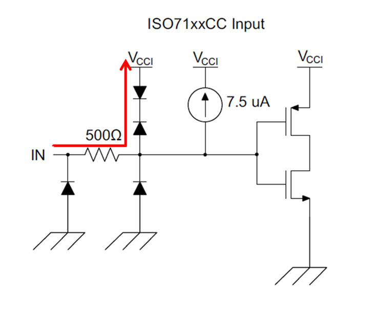
    An input signal will not damage or cause issues with the ISO7141 device. If you look at the simplified device I/O schematics on page 20 of the ISO7141 datasheet you can see there are blocking diodes in each direction. INA having a signal will not damage the part when Vcc1 is powered down. 

    Please let me know if this answers your question or if you have any additional questions. 

    Have a great weekend!

    Best regards, 

    Dan

  • Thanks for your response.  

    According to the maximum ratings. The max for INx is VCC+0.5.   If VCC is 0, and INx is 3.3V logic and HIGH, this will not damage the part? This exceeds the max rating.

  • Hi Nathan,

    Your understanding of INx datasheet spec violation is accurate. Applying 3.3V at INx when VCCx is 0V is going to violate the absolute maximum rating of INx pin hence such operation of ISO71441 is not recommended. Like Dan mentioned, such operation is not going to damage the device immediately. It may affect device's reliability if operated in such conditions for long periods of time.

    We want run a few tests to provide you with more data, please allow us to come back to you mid next week with more information on this. Please note Monday is a holiday in US hence we will be able to come back on either Tuesday or Wednesday. Thank you.


    Regards,
    Koteshwar Rao
  • Dear Nathan,

    sorry for the late reply.

    We used a curve tracer to verify the input schematic.


    The currnent will flow as on the image above from your input through the 500Ohms resistor to VCC.
    The current is limited by this resistor. As my colleagues stated, this wont destroy your device but might degrade it over time. Hence we dont recommend this.

    Additionally it will also depent on the drive strength of your signal source on the input pin. Do you know how much current the output can provide?

    Please let me know if you need further information?

    Best Regards,

    Matthias

  • Thanks for the information, it has been very helpful.   Would either of you have a recommendation for an alternative isolation chip where it would not matter if the inputs are driven when it is unpowered?

  • Hi Nathan,

    The Isolation team has discussed this internally, and although this is a common constraint for isolators we do not have a solution which meets this criteria.

    If you would like to consider other operating scenarios or devices, feel free to ask a related question or create a new thread!

    Thank you for choosing TI parts


    Best,
    Manuel Chavez