This thread has been locked.

If you have a related question, please click the "Ask a related question" button in the top right corner. The newly created question will be automatically linked to this question.

Low jitter clock via a digital isolator

Other Parts Discussed in Thread: ISO721M, ISO7641FM, ADS1271

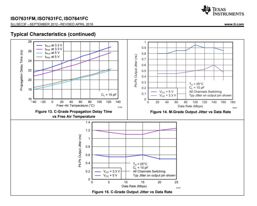
I am looking for a solution to isolate a clock signal used by an ADC. As the sampling clock jitter affect a final ADC performance (SNR) I am looking for as minimum jitter introduced by the isolation barrier as possible. Are the digital isolators suitable for such application? Looking at the fastest TI devices, e.g. ISO721M they introduce jitter as much as 1ns (pk-pk) typical. Are there better performing parts in the TI portfolio? The jitter specification is shown in the documentation for a random data pattern and an NRZ pattern, the second is lower so am I right that for a clock signal it will be further improved?

Thanks,

Robert

ISO721M
  • Hi Robert,

    if your clock is continuous, you could consider AC coupling to get through the barrier.  A suitably rated transformer or capacitor will do the job, depending on your clock frequency.

    You might want to filter the clock on the sending side to a more-or-less sine waveform and bias the output to the threshold of a comparator or line receiver with a logic output to match your ADC.

    You'll need to choose the comparator/line receiver with a bit of care but you should be able to get below 1ns.

    If the voltage across the barrier is AC you'll need to make sure the output circuit isn't sensitive to that frequency range, probably straightforward if your clock is a much higher frequency than the voltage across the barrier.

    Sorry if you've already dismissed that approach as unsuitable....

    Alex.

  • Hi Alex,

    Thanks for your thoughts.

    I initially considered using AC coupling to build the barrier but the barrier must be safety certified at the end (IEC61010-1) so I prefer to stay with the off the shelf certified parts (isolators). For this application the clock range is 2.5MHz-25MHz, the clock is continuous during a normal operation (acquisition) and switched off / changes its frequency between acquisitions, it's not a problem as the ADC needs to be in reset when the clock is not stable anyhow.

    I do not fully understand the idea behind filtering the sending side, what would be benefit of it?

    Thanks,
    Robert
  • Hi Robert,

    It might be tricky to get a wide frequency band across an AC coupling circuit without introducing some distortion to a square waveform. A distorted waveform at the comparator can give you double edges (or worse) at waveform transitions, so a sine waveform might be easier to get a clean clock from.

    If you can get an understanding of the kind of jitter introduced by the isolator, you might be able to filter it out with a phase-locked loop but you would have to be confident the frequency range of the jitter fell outside the loop bandwidth of the PLL. That adds significant complexity to your ADC system but there are devices to help like these www.ti.com/.../overview.html from TI.

    Silicon Labs and IDT do devices of this type too.


    Yours,


    Alex.
  • Hi Robert,

    Thanks for posting your question on our forums.  [Alex,  quick thank you for your responses as well!]

    We do have  devices with < 1ns jitter if that is still of interest.  For example, the ISO7641FM  can do 0.5ns. Please see Figure 14 below [taken from the datasheet] for more details.  Do you have a particular value in mind as a spec target? [with the full understanding here being lower the better]

    Regards,

    abhi

  • Hi Robert,

    • You have a few more options here, the ISO734X family (datasheet) can support even lower jitter (~ 130 ps typ) up to a data rate of 25Mbps.
    • Another datapoint, sharing as an example only:  the following TI Design (link) shows an example of how the ISO7340 is used in a  20-Bit, 1-MSPS Isolator Optimized Data Acquisition Reference Design.

    I hope this helps! I am tentatively marking this as "TI thinks resolved" for now, but please feel free to ask us further questions on this or on another topic- and we'll be here to help out.

    Regards,

    abhi

    PS: Thanks/credit to my colleagues Anant and Sreeram for the discussion on the 73XX and the TI Design referenced above.

  • Thank you Alex. A jitter cleaner is surely another possibility but as it is going to be a multi channel instrument it would need to be replicated multiple times. Anyhow thanks fort your valuable thoughts, you try to approach a problem from different sides.

    Regards,

    Robert

  • Thank you Abhi,

    the part you mentioned looks acceptable. The ADC has not been chosen yet but initially we plan to use ADS1271 so the highest input signal might be 50kHz. To not to ruin the ADC SNR performance I think we need 20ps maybe 50ps of RMS jitter. The part seems to me as suitable. Can I assume that specified pk-pk jitter has a normal distribution? Is there a single channel part of similar performance, I would like to ADC separate the clock from the interface signals. I found ISO7310x but the jitter performance is twice higher.

    I noticed that the ISO7340x has quite wide range of propagation delay, it may be another challenge to synchronize all channels.

    Regards,
    Robert
  • Hi Robert,

    In this case we highly recommend you check out the TI Design link we sent above.

    The impact of ISO7310 jitter on SNR is measured in that design and you can look at the data and see if the SNR is good enough. You may also need to combine the ISO7310 [low jitter] with the ISO77xx parts [higher bandwidth; 100Mbps].

    Hope this helps.

    Regards,
    Abhi