A related question is a question created from another question. When the related question is created, it will be automatically linked to the original question.
If you have a related question, please click the "Ask a related question" button in the top right corner. The newly created question will be automatically linked to this question.
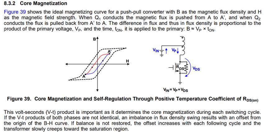
Thank you for using the SN6505 and creating this post on E2E. An SN6505 + transformer system has a margin for normal operation where the transformer is not magnetically saturated (within dotted line in Figure 39) and every time D1 and D2 switch, the operating point moves between A and A' as shown in the illustration.
The SN650x family of devices feature a self-correcting factor where the resistance of output FETs increases yielding a lower voltage seen on the primary side of the transformer, Vp, but v-t imbalances can be prevented in the best way by designing systems so the SN6505 sees balanced loads. This is implemented by using transformers with equal turns above and below the center taps with the appropriate V-t products. For instructions on how to calculate this, please refer to section 9.2.2.5.1 of the device datasheets.
If you have additional questions or would like for me to check a system you are working with, please click reply and let me know! We can also continue this conversation via PM.
Manuel,
you mentioned self-correcting. So you mean that the device could increase the on resistance of Q1 if there is an offset of flux density to the first quadrant of B-H curve? How could the device know that?
My customer is concerned that the devices Q1 and Q2 on time is not 100% identical which will lead to flux saturation.
In datasheet, Average ON time mismatch between D1 and D2 is 0. But it's typical value. It's possible that the turn on time is not well matched and one may always be longer than the other.
My apologies for the delay; I would like to provide as detailed a response as possible, so this may require a follow up post.
Generally speaking, the SN650x self-correcting effect is not from a feedback or closed-loop system. This is only the result of an output FET (or both FETs) heating up due to prolonged on time. If there were a flux density offset where Q1 was on longer than Q2, that FET's operating temperature would increase, leading its drain to source resistance to increase as well, and causing less power to be converted and dissipated by the transformer during that switching cycle. This is only effective to an extent, so it is important to design balanced loads between D1 and D2 cycles.
Internally, the signals controlling the output FETs in the SN650x are complimentary and derived from the same clock source. Since the D1 and D2 signals are exact compliments of each other, any ON time mismatch is negligible. I will inquire about why it is specified this way on the datasheet and respond this week.
Please let me know if there is something for me to elaborate on meanwhile.