This thread has been locked.

If you have a related question, please click the "Ask a related question" button in the top right corner. The newly created question will be automatically linked to this question.

ISOW7821: Isolation between package and casing

Part Number: ISOW7821

My customer has very limited height for the components on their PCB and isolation guidelines need to be followed between the top of package and their casing. The allowed height of components without isolation (towards the package top) is 2.5mm and for components with (at least) basic isolation is 3.0mm. The ISOW7821F has a height of 2.65mm and could only be used if it offers basic (reinforced would be even better) isolation towards the top of the package. 

Thanks

Josef  

  • Hi Josef,

    I am not completely sure if I understand the customer concern completely. I understand from your post that customer needs an isolator with a maximum (or is it minimum?) device height of 3.0mm for basic isolation, I am not sure if they need basic isolation or reinforced isolation and if there is a higher or lower height requirement. ISOW7821F has a height of 2.65mm which less than 3.0mm and hence should meet customer requirement.

    If my understanding is wrong, please do help elaborate your question and customer requirement. Thanks.

    Regards,
    Koteshwar Rao

  • Hi,

    The question is isolation between top of the ISOW7821F package and our casing (we do not talking about internal isolation of the IC). If the top of the package is basic-insulated then we can use the component. Our requirement: if top of the used component is basic-insulated, then it height can be 3mm. if not, then 2.5mm. Height of the ISOW7821F package is 2.65mm

  • Hi Koti,

    to meet isolation guidelines there need to be a certain air gap between the top of the package and the chassis. This air gap can be smaller or larger depending on which isolation ISOW7821F offers towards the top of its package. If there is no isolation that air gap need to be bigger and the maximal possible package height is limited to 2.5mm. However if ISOW7821F offers basic isolation towards the top of package, the air gap can be smaller and the maximal possible package height is 3.0mm.

    If there was reinforced isolation to the top of package the air gap might be even smaller, but this is not relevant here because ISOW7821F fits already within the 3.0mm.

    Hope this helps. 

    Best Regards

    Josef 

  • Hi User5262488, Josef,

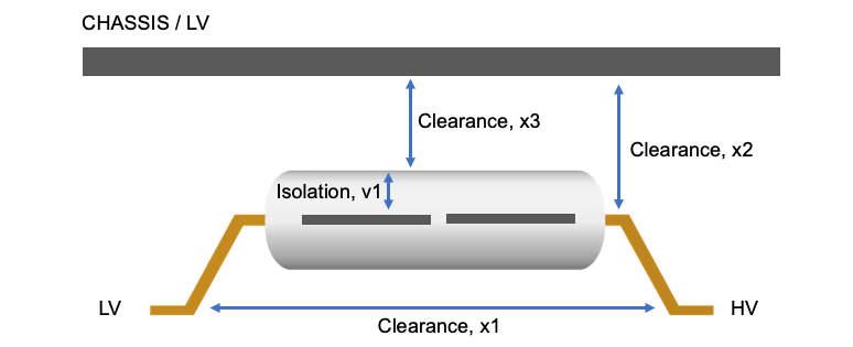
    Thank you for clarifying your question, I think I understand it better now. To make our discussion easier and to make sure we both are on the same page, I have drawn the below illustration.

    The diagram shows side view of the device ISOW7821F where one side of device is on low voltage (LV) while the other on high voltage (HV). The device ISOW7821F supports a clearance of >8mm as stated in the datasheet but I believe the actual clearance requirement of the application between LV and HV is much lower than 8mm based on the HV battery voltage, let's term the application clearance requirement as x1 (shown in the diagram).

    The spacing between the device pins on HV side and the chassis on the top also need to be maintained as per LV/HV clearance requirement to avoid any arcing. Hence, x2 also needs to be maintained to be either equal to or greater than x1.

    From your question, I understand that customer needs to determine x3 based on the isolation level (v1) that ISOW7821F supports. Please do correct if my understanding is incorrect.

    I would like to inform that we do not characterize for v1 and hence, we do not have a value to quote for v1. Since there is mold compound between the die and top of the package, this region is definitely isolated but we do not know what is the isolation voltage that this region supports but can say that this mold compound isolation will be much higher than air isolation.

    Since x2 needs to be maintained to be => x1 to support the LV/HV clearance requirement, I can speculate that the value achieved for x3 by maintaining x2 => x1 already meets the LV/HV clearance requirements. This is due to the fact that there is good amount of mold compound between die and device package top. The isolation voltage supported by die to chassis spacing is expected to be higher than the isolation voltage supported by HV pin to chassis.
    Please note that this is only a speculation and not a claim.

    To conclude, we speculate that if x2 is maintained to be equal to or greater than x1 to meet LV/HV clearance then x3 would have already met the LV/HV clearance requirement. This means that making x2 => x1 would be sufficient for your application and you need not have to look at x3.


    Let me know this helps answer your question, thank you.

    Regards,
    Koteshwar Rao

  • Hi Koti,

    Is there any live parts over 2.5mm height inside of package ? (Package maximum height is 2.65mm)
    If not, then we have no worry to use component on bottom.

    Thanks & BR,
    KF

  • Hi KF,

    Thanks for further clarifying the requirement.

    No, there isn't any active part over 2.5mm height inside of the package. The die and associated connections reside much lower than that and hence no active components at or after the 2.5mm height of the package. Thanks.

    Regards,
    Koteshwar Rao