This thread has been locked.

If you have a related question, please click the "Ask a related question" button in the top right corner. The newly created question will be automatically linked to this question.

ISO1540: How does typical application work

Part Number: ISO1540
Other Parts Discussed in Thread: MSP430G2132

Hi all,

I have read discussion: ISO1540: Customer would like to double check application design

And have a couple of questions:

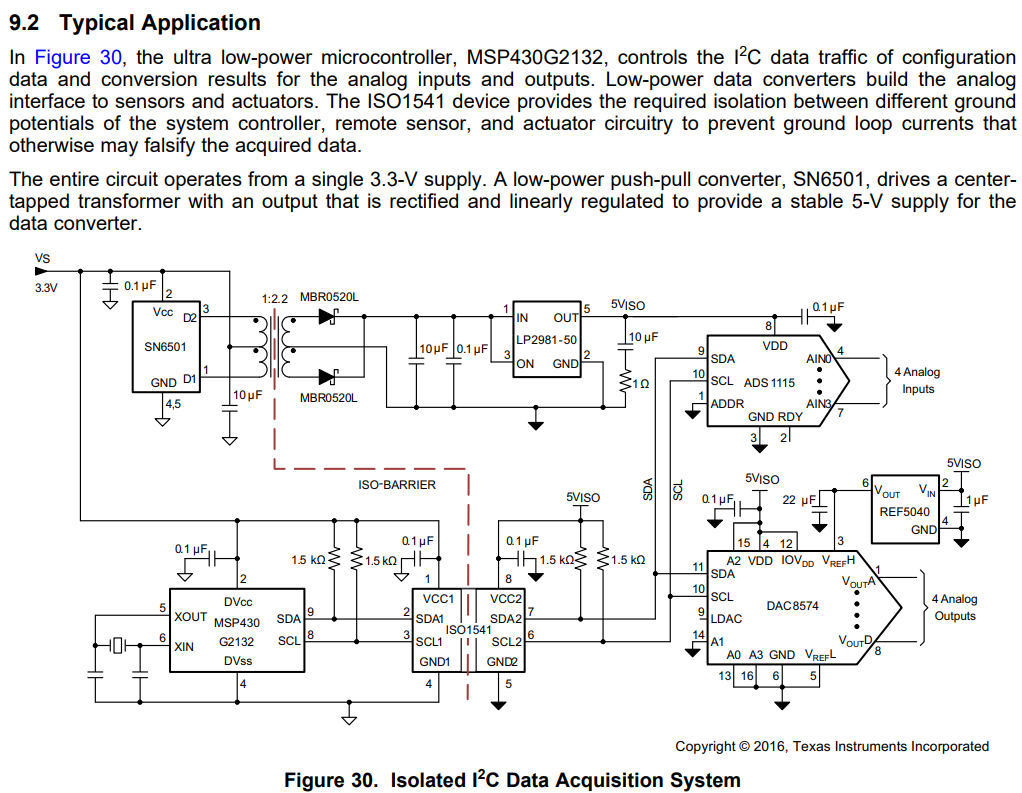
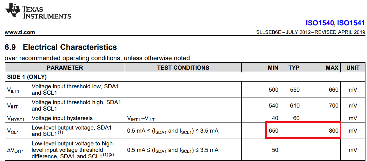
1) Does this mean that in typical application of ISO1540 (first picture below), lowest margin for voltage is 0.025V (825mV - 800mV = 25mV)?

Vol1 = 650mV - 800mV (ISO1540 SIDE1 low output voltage).

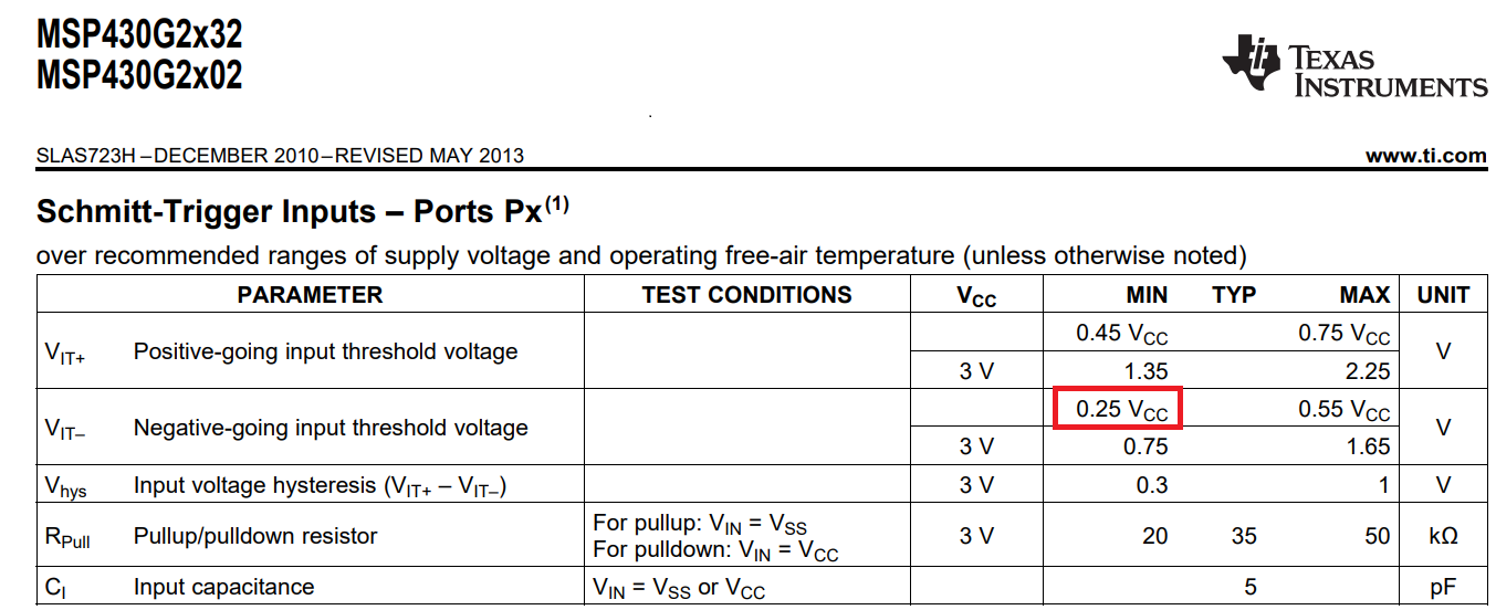
Vit- = 0.25*Vcc - 0.55*Vcc or for Vcc = 3V3 (as in typical application) Vit- = 825mV - 1815mV (MSP430G2132 Negative-going input threshold voltage)

2) Is this enough for reliable operation in temperature range from -40 deg to +85 deg (for example)?

Best regards,

Veljko

  • Hi Veljko,

    Thank you for posting, and welcome to E2E!

    Yes, the V_OL1 spec of 800mV for SDA1 and SCL1 low-level outputs will not be exceeded by ISO154x devices, so 25mV margin is the worst case at Vcc = 3.3V.

    The datasheet specs referenced above apply to both devices across their operating temperature ranges, so this margin is the worst case across -40dC to +85dC temperatures.

    A concern to check is the power supply level on MSP430G2132, since V_IT- will scale proportionally with Vcc. If the 3.3V rail falls to 3.2V, margin between V_OL1 and V_IT- reduces to 0mV, so it will be important to properly decouple the power supplies on each IC, and if transients are expected to reduce the power supply level for long amounts of time, possibly increase the supply voltage.

    Please let me know if you have any feedback or comments.


    Respectfully,
    Manuel Chavez