A related question is a question created from another question. When the related question is created, it will be automatically linked to the original question.
If you have a related question, please click the "Ask a related question" button in the top right corner. The newly created question will be automatically linked to this question.
Part Number: SN6505B Other Parts Discussed in Thread: SN6501
Is it possible to have two SN6505B parts in parallel (One on top of the other one)? They will be sync with the same CLK. We want to do this because the current limiting sometimes kicks in.
Did you mean to ask if the outputs of two SN6505B based power supply solutions can be tied together to increase the power? Or did you mean to ask if two SN6505B devices can be connected in parallel to a single transformer to increase input current support?
The answer is NO for both of these questions. The devices do not have any features to allow them to be connected in parallel and the external clock option is only to help customer choose the switching frequency to the value of their interest to aid them in managing emissions better. Thanks.
I'm not too sure what is the difference between the two option questions you give me. The second question seem closer to what I want to do. Having two SN6505B devices, I want to connect D1 of device 1 to D1 of device 2 and D2 of device 1 with D2 of device 2. and both D1 and D2 each go to the transformer.
If the answer is NO, then can I drive external FETs with a single SN6505B (D1 going to a gate of FET1 and D2 going to a gate of FET2) or is there another way to increase the power?
As Koteshwar mentioned, connecting the D1 and D2 pins of two SN6505 (or SN6501) devices is not recommended because they are not designed to divide current loads between multiple devices. The part-to-part variation in switching characteristics could lead to damage of any two devices connected in parallel.
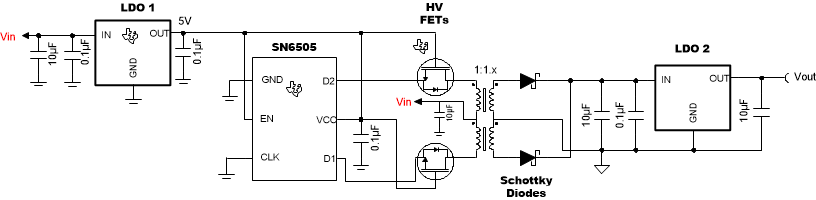
External FETs can be included as shown below to increase power capability of the isolated supply, however this solution increases voltage capacity on the primary side, not current-sinking capability:
For the solution above to boost current, Vin would need to be greater than Vout and the transformer would need to have a turns ratio < 1 (step-down transformer). What is the maximum load current this solution needs to supply?
We connect the SN6505 to a battery pack which can go as low as 2.9V and our Vout after the LDO 2 in your schematic needs to be kept at 3.1V.
Is there a way to boost the Iout current at Vout when Vin is lower than Vout?
We will be okay at the Vout side, if we can get 150mA more current from our existing design when Vin is 2.9V . Our existing design looks exactly as your schematic, just substitute the LDO1 with a 4.2V battery pack and connect the D1 & D2 directly into the transformer without the HV FETs. The LDO 2 outputs 3.1V.
Thank you for providing the additional design information. Our team is continuing to discuss potential solutions, and I expect to follow up on that early next week. Meanwhile, please confirm whether an external CLK will be used for this SN6505 system or if the internal CLK of SN6505 will be used.
Thank you for your flexibility here. Our team had considered connecting SN6505 devices in parallel with an external CLK, however even then there is a concern for unintended D1 / D2 short-circuits.
A final idea we are considering is using SN6505 to drive the gates of external FETs capable of sinking >1A. Please allow us until the end of this week to conclude this conversation and share our findings.
Let us know if there is additional support we can provide meanwhile.
The topology we've considered to drive >1A using SN6505 is shown below:
V1 can be operated by 3V, but the external N-channel FETs will need to have a Vgth much lower than this and be capable of sinking >1A. How much current will be needed is unclear, but a FET like SSM3K329R should work.
This design does come with the tradeoff that some features of SN6505 will be lost on the external FETs, like current limit and thermal shutdown.
Please let me know if this is a solution for you to consider, otherwise the the isolated load could be divided between two independent SN6505 power supply circuits.
Thank you, and have a great weekend, Manuel Chavez
Thank you for your response. I'm building a test board to test both configurations. This one (FET Driven) and the parallel (Two SN6505B in parallel). Should I connect diodes from the drain of the FETs to the center of the transformer to reduce EMI? Or the diodes are going to screw up the transformer performance? Like this:
You're welcome! To clarify, does the configuration you are building with two SN6505B in parallel share ground connections but separate the isolated power supply rails?
The SS24T3G diodes in this schematic would prevent push-pull operation of the SN6505 and transformer as explained in the following posts. These diodes and the Schottky diodes used could also affect performance negatively if ambient temperature exceeds ~85dC, when maximum reverse leakage current increases substantially and could lead to a collapse of the power supply similar to the case mentioned in this E2E thread.
How will these diodes reduce EMI? This is a technique i am not familiar with and would like to learn more about.
The configuration we are thinking uses the same power rails as well. It is like connecting a second SN6505B on top of an existing one.
Thank you for the tip regarding the diodes temperature.
Now regarding how the diodes can reduce EMI... I don't know if this is the case with transformer coils but when the FETs opens, the voltage of the primary coil will be reversed and this primary coil voltage is going to be added to the V+ power supply voltage and therefore the FETs Vds voltage is going to be the power supply plus the reverse voltage of the primary coil (Maximum twice the power supply 2 * V+). And this means more current when the FET closes. In the other hand, if we connect a diode in parallel with the primary coil, the reverse voltage of the primary coil will be drain to the V+ of the power supply and therefore the FETs Vds maximum voltage will be the power supply voltage plus the diode's forward voltage (Power supply plus 0.6V). Then the FETs Vds is not as big and therefore it will reducing the EMI produced when the FET switches on and off). But again I don't know if this is the case with transformers. Please correct me.
You're welcome, and the configuration of two SN6505B devices in parallel may work experimentally, but we cannot guarantee that the devices will not be damaged or that their long-term reliability won't be affected hence we do not recommend it.
Regarding the diodes, thank you for the explanation. The voltage increase of the primary coil above V+ power supply voltage is necessary for the center-tapped transformer to operate properly. This is described in Section 8.3.1 of the SN6505 datasheet (image below):
On this note, using diodes from D1/D2 to V+ will affect the push-pull operation; please do remove these diodes from the design and I will update my previous response to reflect this.
RB168MM-40 are recommended Schottky diodes to be used on the output of the isolated power supply if ambient temperatures are expected to exceed 85dC. For other cases, we recommend MBR0520L.
Other methods to mitigate EMI are to select transformers with low leakage inductance or to design placeholders for a snubber circuit on D1/D2 pins as shown below: