This thread has been locked.

If you have a related question, please click the "Ask a related question" button in the top right corner. The newly created question will be automatically linked to this question.

SN6505B: Protecting the transformer from overcurrent

Expert 1961 points
Part Number: SN6505B
Other Parts Discussed in Thread: TPS25200, SN6501, INA180

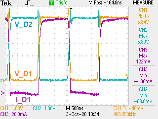
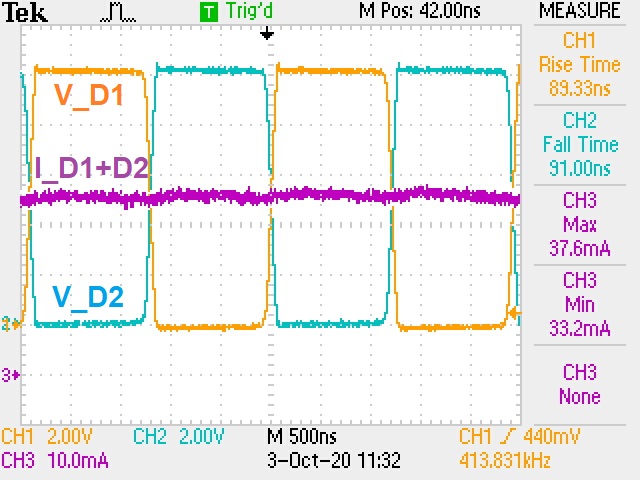
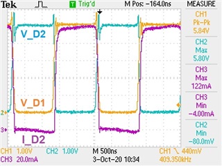
The SN6505B has a current limit of 1.7A, which will protect the SN6505B from burning up.  But isn’t that too high of a value to protect the other elements of the circuit such as one of the small 100 mA Wurth transformers? Is that current limit only useful when using one of the 1-Amp transformers?

I’ve considered using other current sense devices to protect the entire circuit (such as an eFuse), but I think I need to understand how the SN6505B's current limit works before discussing other options.

Thank you for the help!

Regards,

Greg

  • Hi Greg,

    I believe you are in discussion with Manuel on various topics related to SN6505B.Your understanding is correct, the current limit spec'd in datasheet is primarily to protect the device SN6505B from damage. Since the device doesn't have access to the output side of circuit, it cannot really know the output currents and hence achieving current limits for outputs won't be possible by SN6505B without any additional circuitry.
    Using external current limiting or protection devices like eFuse is the right approach to limit currents and protect other components and loads.

    I will also let Manuel add his inputs if there is more to add. Thanks.

    Regards,
    Koteshwar Rao

  • Hi Koteshwar,

    Oh oh, sounds like I have a reputation for asking questions!  I'm glad I'm in question-friendly territory.  Manuel has been very helpful, as I can tell you are too.

    Until the e2e forum has the feature of original threads having links to "Ask a related question" threads, I'm still going to bundle my questions somewhat.

    Thank you for answering my question about the current limit of the SN6505B.  I'm glad that it protects itself.  I understand the desire to retain compatibility with the SN6501, so the package needed to stay the same.  The package only has 6 pins and so there isn't room for an "ILIM" pin, which would be a great addition.  "CLK" and "EN" were added as features, so there isn't room for "ILIM".  An eFuse like the TPS25200 has a pin for setting the current limit of the device by connecting a resistor from this pin to ground.  If you are working on new push-pull drivers, please add that as a feature request for a new device.

    VCC connects to the center tap of the primary of the transformer.  What is the nature of the current through this node?  I assume it is somewhat of a square wave given the way the two transistors alternately pull current through each leg of the primary, kind of like milking a cow ;-).  But the waveform of the current could have some spikes to it, making it problematic to measure with a current-sensing device like the eFuse.  How well behaved is it?  Could there be spikes of current that would trip the eFuse that supplies the 5V to the transformer and SN6505?  If so, my 2nd approach would be more intelligent, and would involve a current sense such as the INA180 and a microcontroller.  Using an external clock signal would make it easier to position the A/D sampling of the current sense.  Perhaps a discrete analog comparator circuit could be used instead of a microcontroller, though a microcontroller would be a good source of a clock for that circuit.

    Please let me know your thoughts on protecting the circuit using an eFuse or current sense amplifier.  Would an eFuse be a reliable method?  Thanks for the help.

    Regards,

    Greg

    VCC

  • FYI, the "VCC" at end of my post is not supposed to be there.  It happened when I copied it from Word in order to get the subscript formatting.  It isn't supposed to my signature, so don't interpret it as my title or something like that.

    Greg

    VCC

  • OK, it happened again, and it wasn't there when I clicked Reply.  This time I will click the "Paste from Word" button.  Here goes: VCC

    If it still does it, I won't worry about it.

    Greg

  • Hi Greg,

    No worries, and thank you for the feedback for TI's future products!

    There will be some transients in the power supply, like during load-change or power-up/down conditions, but these are more gradual with SN6505 than with SN6501 due to it's "soft start" mechanism.

    Current limits with an eFUSE might be the simplest to implement, and we do expect it to be a reliable circuit protection method; regardless of which protection circuit is implemented, please do ensure that it allows sufficient current to pass for normal operation along with margin for expected transients while protecting the circuit.

    For your reference, below are some waveforms showing the relationship of switching voltage and current waveforms in SN650x devices. These waveforms were captured in a Test Circuit configuration, shown by Figure 6-4 in the SN6501 datasheet:

    Current through D1/D2 pins waveforms by themselves:


    D1/D2 voltage waveforms with D1 current in-line (D2 current would be the same as D1 current but 180 degrees out of phase):


    D1/D2 voltage waveforms with combined D1/D2 current (i.e. the Vcc current):


    Hopefully this is helpful!


    Respectfully,
    Manuel Chavez

  • Hi Manuel,

    Thank you for the nice scope traces.  I see that the test circuit uses a resistive load, not an inductive one.  Would there be much more ringing when driving the transformer windings? I noticed that the current does not ring like voltage does, which is good because that is what I need to measure.

    In the first trace it shows channels 3 and 4 as 100 mA per division. This is consistent with where the arrow is pointing in the lower right corner, which looks to be about 44 mA. The numbers aren’t making sense to me. If it is a SN6501, the current of about 480 mA is well beyond the max rating of 350 mA. With a 5V supply and a 50-Ohm resistor, the maximum amount of current that should flow is 5/50 = 100 mA. If there is an issue with a 10x probe, dividing the 480 mA by 10 doesn’t solve the problem either, because then the voltage would only be 0.048 x 50 = 2.4V.

    The second trace makes more sense. The voltage for D1 and D2 are 1V per division, and so the waveforms are nominally 5V which is what I would expect. The current is pretty close to what I would expect (5/50 = 100 mA), but it isn’t exact so I’m wondering why not? Why does I_D1 go negative when the MOSFET is off?

    In the third trace, why did the volts/division change to 2V? That means the p-p voltage is 10V. Why wouldn’t I_D1+D2 equal something closer to 100 mA? While the numbers are not making sense to me, the I_D1+D2 waveform looks great! No glitching when switching between D1 and D2.

    Do you happen to have any scope plots of the circuit in Figure 6-1 or 6-3 with a load?

    I’m probably missing a key piece of information and the graphs are fine.

    In general, it sounds like the eFuse would work pretty well since the current appears to be well-behaved. I’m having a little trouble understanding the details of the scope plots though.

    Regards,

    Greg

  • Regarding the future product suggestion, it occurred to me that adding a current limit feature to the SN6505 would have required more than just a single ILIM pin, since the current for the transformer does not flow through the SN6505. So you would need to add a Vout pin too since the device already would have a VCC pin.

    In a previous design I used an LDO on the output of the transformer. The LDO had foldback protection, which means that beyond 250 mA the LDO would limit the current to that value and reduce the output voltage. That worked well at protecting all of the components in the SN6501 circuit, but in general, I’m questioning if that is a good reaction to the fault. Operating at a reduced voltage could result in some squirrely behavior. I’m beginning to think now that it would be better to turn off the output completely. Whether it is auto-retry or latch-off behavior is another question. I lean towards latch-off, but others might prefer auto-retry. Any thoughts on this?

    The fancy voltage clamping features of the eFuses could be omitted, since an eFuse in this application is more likely to use stable system power. All it needs to do is detect an overcurrent situation.

    This is just a wish list of features. In the meantime, it certainly looks like adding an eFuse will do a great job of bullet-proofing the design.

    Regards,

    Greg

  • Hi Greg,

    Thanks for following up! Please regard these waveforms as separate tests of SN6501 and SN6505B. They were each captured under slightly different conditions and do not represent the same conditions from one image to another -- I shared these so that you could visualize these waveforms' general relationship.

    The voltage waveforms will likely show ringing during switching when the transformer is connected and at heavier loads. How much ringing appears is dependent on the transformer, layout, and operating conditions; in general both the current and voltage waveforms will follow the waveforms above across operating conditions, with the exception that the switching voltage waveforms will swing between 0V and 2x Vcc due to push-pull action of the transformer.


    Have a great weekend,
    Manuel Chavez

  • Hi Manuel,

    Looks like e2e got a makeover!  I’m looking forward to seeing what has changed.  It has been a while since I last posted.  Life kind of flew past me.

    I'm sorry for taking the plots too literally with respect to the test circuit and an SN6501.  Knowing that some were taken with an SN6505, that explains the excessive current.

    You said "D1 current in-line" for the 2nd trace.  Does that mean the current through the drive transistor on D1?  Do you know what causes the negative current in that plot?  The voltage waveforms are 0 to 5V in that plot, so I assume that test configuration is with resistors?  And the 2x voltage in the 3rd plot suggests that test included a transformer?

    Regards,

    Greg

  • Hi Greg,

    It sure did! Hopefully you find some pleasing upgrades to the site Slight smile

    No worries about the plots! We're glad to add context or provide any additional information to help out. About the D1 current being "in-line" with the voltage waveforms in the 2nd plot, I meant the voltage and current waveforms for D1 were in-phase visually, but this is a mistake. The current and voltage for D1 (or D2) should be out of phase since no current flows when the transistor is OFF. My apologies; a corrected plot is shown below:


    The slightly negative current is an artifact of the measurement here, and we don't expect negative current to flow from the test configuration used. In a typical application, there might be some negative current or voltage ripple when D1/D2 is switching due to parasitic impedances in the transformer or layout.

    Yes, the third plot was captured with a transformer in the typical configuration.

    Please let us know if there is further information we can provide!


    Thank you,
    Manuel Chavez

  • Hi Manuel,

    Thank you for the updated plot.  That makes sense.  Glad to know that the negative current was a measurement artifact!

    In the SN6501 datasheet, Figure 8-10 is not a good circuit to use because it could lead to a core magnetization problem if the outputs are asymmetrically loaded.  Here is that circuit:

    The problem with that circuit is that Vout+ is only sourced by D1, and Vout- is only sourced by D2.  Figure 8-8 is bipolar like Figure 8-10, but it is OK because the full secondary is used for both D1 and D2.  Each driver simultaneously charges both capacitors.  The other two circuits are OK because they are unipolar.  D1 and D2 contribute to the same output.  I reported this a while back and it was agreed that it was a problem.  The SN6501 datasheet wasn't changed, though that circuit wasn’t included in the SN6505 datasheet.

    Regards,

    Greg

  • Hi Greg,

    You're welcome! Thanks for bringing this up -- can you please share the prior communication about the circuit in Figure 8-10 over Personal Message?


    Thank you,
    Manuel Chavez

  • Hi Manuel,

    Sure!  I'll look for it.

    Regards,

    Greg

  • Hi Greg,

    Thanks! We can update this thread accordingly following our conversation.


    Thank you,
    Manuel Chavez

  • Hi Greg, all,

    Greg kindly shared his earlier message with TI about the circuit in Figure 8-10 above. The circuit requires balanced loads across both outputs to help prevent saturation of the transformer, and TI decided not to remove the circuit from the datasheet neither earlier nor at this time.

    If there are any follow-up questions regarding this or any other circuits using SN650x devices, please feel free to "Ask a related question" or "Ask a new question" using the yellow and red buttons in the upper right corner of this window.


    Thank you,
    Manuel Chavez

  • Thank you Manual.  I don't have a follow-up question, but I would like to add some thoughts on the matter.  I don't have an issue with the circuit being in the datasheet because it will work if the loads are balanced.  But I have a concern about how much imbalance is needed to cause the transformer to be saturated.  My recommendation is to add a note in the datasheet that says "To avoid core saturation, the loads in the circuit should be balanced in order to maintain a balanced V-t on the primary".  In my opinion, this problem isn't obvious when looking at the circuit, and so I would expect most people to use it without knowing there is a limitation.  It wouldn't be uncommon to run a lot of circuits off the positive rail and a minor amount off the negative rail for an analog front end.

    Regards,

    Greg

  • Hi Greg,

    Thanks! We will consider adding a note to the datasheets in the next round of updates.


    Respectfully,
    Manuel Chavez