This thread has been locked.

If you have a related question, please click the "Ask a related question" button in the top right corner. The newly created question will be automatically linked to this question.

SN74LVC244A: SN74LVC/SN74CBT/LSF

Part Number: SN74LVC244A
Other Parts Discussed in Thread: SN74CBTLV3245A

Dear,

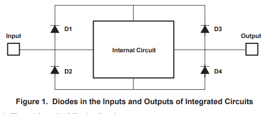
    I have read the document"SDYA012",and found that every integrated circuits have diodes at input and output;so what's about SN74LVC/SN74CBT/LSF devices? whether they also have input/output diodes?The reason i focus on it is that i want to know whether the current will flow backward when live inserting;

  Pls help me to verify it ,Thanks!

  • Some devices (e.g., LVC/LSF) do not have positive clamping diodes at their inputs. See [FAQ] Can the input voltage (Vi) to my logic device be higher than the supply voltage (Vcc)?

    Some devices (mostly devices with open-drain outputs) do not have positive clamping diodes at their outputs.
    Some other devices block backflow currents when powered off; see [FAQ] What does 'partial power down' or 'Ioff' mean in the datasheet?

  • Hi ,

       Sorry to disturbing you again,I'm still puzzled about some points:

    1.the figure 1 at "SDYA012" and"scea026",The D3 in "SDYA012" is the clamping diode and it's not the same one as described parasitic diode at "scea026";Not sure if I am understanding this right;

    2.About the blocking doide,take the bus switch 74cbtlv245 for example;according to  [FAQ] Can the input voltage (Vi) to my logic device be higher than the supply voltage (Vcc)?,the input has no clamping diode;according to "SDYA012",the 74cbtlv245's output is open-drain,so the D3 is absent,but i still don't know whether it has blocking diode  or not;In my opinion, it's bipolar device,and not applyed to "scea026"'s figure1-Totem-Pole Output;Am I right or wrong?

    I'd appreciate it if you help me clarify my doubt,Thanks;

  • 1. These two figures show different devices. All MOSFETs have these parasitic diodes. In most cases, one of them is shorted by a connecton between body and source. In devices With Ioff, the diode is not shorted, which prevents the other diode from having any effect.

    2. A device named "SN74CBTLV245" does not exist. Anyway, the datasheet will tell you whether a device has Ioff.

  • Ji_qiu,

    1.the figure 1 at "SDYA012" and"scea026",The D3 in "SDYA012" is the clamping diode and it's not the same one as described parasitic diode at "scea026";Not sure if I am understanding this right;

    You are correct in your thinking. The parasitic diode is something inherit to all MOSFETs. The D3 diode is a positive clamp diode used as protection.


    2.About the blocking doide,take the bus switch 74cbtlv245 for example;according to  [FAQ] Can the input voltage (Vi) to my logic device be higher than the supply voltage (Vcc)?,the input has no clamping diode;according to "SDYA012",the 74cbtlv245's output is open-drain,so the D3 is absent,but i still don't know whether it has blocking diode  or not;In my opinion, it's bipolar device,and not applyed to "scea026"'s figure1-Totem-Pole Output;Am I right or wrong?

    The blocking diode is used for Ioff and the isn't dependent on the output structure. There isn't a device called SN74CBTLV245. You seem to have mixed some acronyms up. CBTLV is a family in the multiplexers family but the 245 suffix is common in the logic portfolio.
    Nonetheless, the datasheet indicates Ioff. If you see the spec in the datasheet, it supports this features. Usually it will be listed in the features section as well.

    Thanks,
    Rami

  • Hi Rami,

        I'm sorry to mistake the PN,the correct PN is SN74CBTLV3245A and it also support Ioff,but it is FET bus switch,if it suitble to apply the figure1 of "scea026"?Is there blocking diode between VCC and output of SN74CBTLV3245A? 

    Thanks,

     Ji

  • Hi ,

        I'm sorry to mistake the PN,the correct PN is SN74CBTLV3245A and it also support Ioff,but it is FET bus switch,if it suitble to apply the figure1 of "scea026"?Is there blocking diode between VCC and output of SN74CBTLV3245A? 

    Thanks,

  • Ji,

    There will be some circuitry for Ioff protection to protect the system. Scea026 wouldn't quite be the proper figure for this. The inputs of a logic device go into the FETs of the gate while the control pins of switches and muxes would go into gate and the inputs and outputs would the drain/source. Here's a snippet from a TI Precisions lab video that may help about electrical overstress of switches and muxes. This doesn't show Ioff circuitry.

    I'm looping in the switches & multiplexer team to help further expand about the SN74CBTLV3245A I/O diodes and powered off protection circuitry of the SN74CBTLV3245A.

    Thanks,
    Rami

  • Hi Rami,

      Is there any update for I/O diodes and powered off protection circuitry of switches & multiplexer such as SN74CBTLV3245A?I would really appreciate it if you share these points with me;

    Thanks!

  • Hi Ji,

    I am going to sync with our design team on this inquiry and will respond back shortly.

    Thanks!

    Bryan

  • Hi Ji,

    So for this device (and other devices that feature powered off protection), there will be circuitry on the input pins that enables the device to be able to protect itself against input voltages that go above the rail (but not above the abs max). While there will not be a traditional ESD structure as described above with just an ESD diode between the input and VCC, this powered off protection circuitry also incorporates ESD protection as well.

    Thanks!

    Bryan