This thread has been locked.

If you have a related question, please click the "Ask a related question" button in the top right corner. The newly created question will be automatically linked to this question.

SN74LVC2G07: Glitch Consult

Part Number: SN74LVC2G07

Hi Team,

 Could you pls see below question description. There are detailed waveform screenshot attached. Thanks

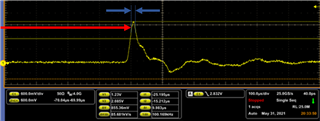
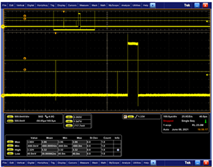
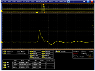
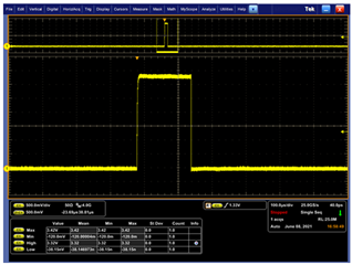
  1. Customer found there is crosstalk glitch at the IC input, but there are no spike at the output side. They want to know what the conditions the crosstalk glitch may cause the IC output falsely. You can see the some spikes reach the Vih(2V) here.

Best,

Stanley

  • Hi Stanley,

    For reference, this is directly related to the issue here: (+) SN74LVC2G07: Tsu and Th specification consult - Logic forum - Logic - TI E2E support forums


    In your scope shots I only see one waveform - I need to see the input and the output together.

    Also, can you provide a schematic? This is an open-drain device, so I need to know the pull-up resistor strength, and it would be helpful to know the loading (trace length and/or total load capacitance).

    To give you some information on how this device works -- it's open-drain, so the output is only pulled _low_ by the SN74LVC2G07. This means that the rising edge is entirely dependent on the external circuit. If you have, for example, a 10 kΩ pull-up resistor to the 3.3 V supply and a typical 50 pF load, then the rising edge at the output will be approximately t_r = 2.2 * 10e3 * 50e-12 = 1.1 μs.

    From the provided scope shot, it looks like the signal exceeds the threshold voltage of the device (1.65V, red arrow) for approximately 0.5 ns, which wouldn't be enough time to cause any variation in the above described output. Please correct me if I'm wrong - it looks to me like this is a zoomed view that is showing 50ns total.

    For an open-drain device, an input glitch of even 10 or 20 nanoseconds won't typically result in a state change at the output just because of how the output works.

  • Hi Emrys,

    Thanks for reply. I need to check customer about the schematic. You know some customers are quite confidential about this part since E2E is public stage. 

    From your above saying, as long as the duration time of input glitch smaller than the rising edge at the output, the open-drain device should have time to flip output state. Pls correct me if I misunderstand it. Thanks.

    Best,

    Stanley  

  • Hi Stanley,

    You know some customers are quite confidential about this part since E2E is public stage. 

    You can create an internal E2E thread that will not be visible to the public if you need assistance on something proprietary or sensitive.

    as long as the duration time of input glitch smaller than the rising edge at the output, the open-drain device should have time to flip output state.

    I would recommend to keep any 'glitches' much shorter than the output rise time. If an input glitch were the same width as the output rise time, then the output would have time to rise & thus propagate the glitch.

    Here's an example simulation with a slow output and a two input pulses - one that's the length of the output rise time, and one that's much shorter:

    To avoid any down-stream devices from receiving the pulse, the voltage should stay well below Vcc / 2.