This thread has been locked.

If you have a related question, please click the "Ask a related question" button in the top right corner. The newly created question will be automatically linked to this question.

LSF0108: B channel logic are transistor issue.

Part Number: LSF0108

Hi,

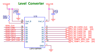
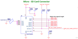
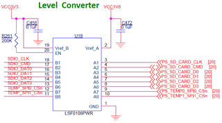
We are using a level converter (LSF0108PWR) to convert 3.3V (Vref B) to 1.8V (Verf A) able to measure the channel A signals logic voltages are 1.8V. But in Channel B signal logic voltages is 2.1 instead of 3.3V for B6, B7, B8 signals and the rest of the B1, B2, B3, B4, B5 channel signal logic voltage is 1.8V instead of 3.3V.

And When I connected EN (low)  to GND, The channel B signal logic voltages are 3.3V for B6, B7, B8 signals and the rest of the B1, B2, B3, B4, B5 channel signal logic voltage is 0V instead of 3.3V.

Please verify the below schematic and suggest if any changes are required.

Regards,

Gajendiran A

  • Hey Gajendiran,

    I see that your biasing circuitry is slightly incorrect and I don't see any pull-ups. I recommend watching the training series on the LSF family. They will greatly help you properly implement this level shifter into your system. Let me know if you have any additional questions after watching the videos.

  • Hi Dylan Hubbard,

    Thank you for the reply, Both Channel A and Channel B all signals ports are required pull resistors that's device side(SD card connector) and FPGA side ? or only either one side is sufficient (A port signals or b port signals) please confirm.

    In currently pull-up resistors(Port-A signals) are enabled on the inside of the FPGA and no pull resistors are used in port B side (SD connector side).

    Please confirm which are signals required pull-up resistors on port A signals and port B signals?

    Note: All signals are not open-drain pin on the level converter.

    Regards,

    Gajendiran A

  • All LSF outputs are open drain. (See the videos.)

    You should have pull-up resistors on all LSF pins used as outputs.

  • The SD card data 0-3 signals are bidirectional pin (IO) even these signals are required pull-up resistors? for both Channel A and B side?

  • Bidirectional pins are output pins, so they need pull-ups.

  • For the bidirectional signal, both side's pull-up resistors are required, right? (port A and port B ).

    If we are not using a pull-up resistor what will be the impact on the design? (Some interfaces are working without pull resistors)

  • Hey Gajendiran,

    For push-pull bi-directional signals, you can get away with not having pull-ups on the lower voltage side (A side in this case). As mentioned in the Down Translation video, this depends on the leakage current of the interfacing device on the A port (<1 uA). The higher voltage side will always need pull-ups to achieve the up translation. Any signals that are open-drain coming from the SD card (lower voltage side) will need pull-ups to drive High. I believe that would only apply to the CMD line, but I'm not fully experienced in SD card interface so I would double check.

  • Hi Dylan Hubbard,

    Thank you for the reply, Did you get chance to look into SD interface ? like how the pull resistors need to configure?

    Can you please suggest which are signals needs pull-up resistors on both the side (A and B) of level convertor?

  • Did you get chance to look into SD interface ?

    Hi Gajendiran,

    It's up to you to look into the requirements for your system -- we can't design it for you.

    Dylan has provided more than enough detail on the LSF, I think you need to learn more about the other devices in your system to make the determination of what pull-up resistors to use.

    If you are incapable of doing that (perhaps the data isn't available), then you can just put pull-up resistors on both sides for all pins and test the board after it's built. You can always adjust a resistor's size or remove it entirely, but it's very difficult to add one back onto the board if it was completely removed from the design.

  • Hi Maier,

    Thank you for the your support!!!

    We have added to pullup resistor for the high side (typically B-side) output signals ( i,e SD clock and CMD) and matched as per datasheet.

    and push-pull, bidirectional signals(SD card data signals) are required pull resistor on high side (typically B-side)?

    Regards,

    Gajendiran A

  • and push-pull, bidirectional signals(SD card data signals) are required pull resistor on high side (typically B-side)?

    Yes, all outputs on the high-side of the device require a pull-up resistor.

    If the LSF is only receiving inputs from a push-pull device on the high side (B port), then there is no need for a pull-up resistor.

  • Thank you for the updated.

    In the LSF datasheet, The continues channel current is 128mA in absolute maximum ratings table. This 128mA is per channel current rating or Channel A and Channel B current rating or Overall channel current rating?

    The current design Vref_B pin directly connected to the 3.3V supply without 200K resistor. So without resistor what will be impact ?

    For the bidirectional signal (Data signal ), pull resistor are enabled on internal to the FPGA that is A side and is it okay if not used pull resistor on B side?

  • Yes, leaving out the 200k resistor is completely incorrect and the device won't function as expected. The short circuit produce will likely also damage the component and possibly other parts of your circuit.

    Please see the video on how to bias the device, located here: Understanding the Bias Circuit for the LSF Family | TI.com Video

  • Sorry forget to mention, we used 200K resistor for enable signal alone but Vref_B pin directly connected to the 3.3V supply will this affect the functionality. Please refer the below image.

    understand that, short circuit produce will likely damage the part.

  • At the EN pin only, the 200 kΩ is useless; it is required to limit the current flowing into Vref_B and out of Vref_A.