This thread has been locked.

If you have a related question, please click the "Ask a related question" button in the top right corner. The newly created question will be automatically linked to this question.

SN74LVC1G125: SN74LVC1G125(6)DBVR

Part Number: SN74LVC1G125
Other Parts Discussed in Thread: SN74LVC1G17, SN74LVC1G99, SN74LVC1G14, SN74HCS125

Hi team,

Regarding SN74LVC1G126DBVR and SN74LVC1G125DBVR, can you help me answer the following questions? Thanks!
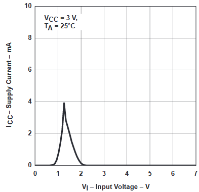
1, Regarding the turn-on level threshold of OE of SN74LVC1G126DBVR:

As shown in the figure above, the power supply is 3V, and the A input of SN74LVC1G126DBVR is directly grounded. When the input level of OE rises from 0, it should be at least 2V to turn on and output 0, but the actual measurement is about 1.36V and the output is 0. I don't know what is the reason?

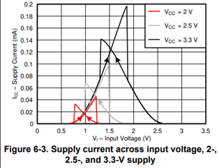
2, About SN74LVC1G125DBVR/OE turn-on level threshold_01:
As shown in the figure above, when the /OE of SN74LVC1G125DBVR starts to rise from 0, does the output turn off when it rises to 0.8V (output high impedance), or does it need to rise to 2V before the output turns off (output high impedance)?

3. About the intermediate state of SN74LVC1G125(6)DBVR:
When input A is standard 0 or 3V and OE is between 0.8V and 2V, what will be the output? How much will the power consumption increase at this time? Will it damage the IC?
When OE is turned on and input A is between 0.8V and 2V, what will be the output? How much will the power consumption increase at this time? Will it damage the chip?
What will the output be when both OE and input A are between 0.8V ~ 2V? How much will the power consumption increase at this time? Will it damage the chip?

Thanks a lot!

Thanks & best regards,

Wendy

  • For voltages above VIH, the input is high. For voltages below VIL, the input is low. For voltages in between, the state of the input is not guaranteed (it might be low, or high, or in the worst case oscillate). Typically, the actual switching threshold is near VCC / 2.

    For the typical power consumption, see below (there is no guaranteed upper limit). To prevent damage, the input voltage must no stay between VIL and VIH for longer than a few nanoseconds; see [FAQ] How does a slow or floating input affect a CMOS device?

    If you need to handle slow signals, put a Schmitt-trigger buffer (e.g., SN74LVC1G17) before the input, or use a device with integrated Schmitt triggers (e.g., SN74LVC1G99, or any SN74HCS device). But a logic gate with Schmitt-trigger inputs does not reduce the power consumption; for that, you would need a comparator.

  • Hi Clemens,

    Thanks for the reply. Since the current signal may stay at the mid-level for a long time, I would like to ask whether the device with Schmitt trigger input can completely avoid this problem (the output is uncertain and the power consumption increases)? If so, can you recommend SN74LVC1G126DBVR and SN74LVC1G125DBVR corresponding replacement with Schmitt trigger? In addition, can you recommend an inverter with Schmitt trigger?
    Another question is, if a comparator is used in the front, can the problems caused by the input intermediate level (the output is uncertain and the power consumption rises) can also be completely avoided?

    Thanks a lot!

    Thanks & best regards,

    Wendy

  • Hey Wendy,

    A schmitt-trigger device will reduce the power consumption, but it will still be higher than having the voltage at VCC or GND. The SN74LVC1G17 is a good choice for a Schmitt trigger buffer and the SN74LVC1G14 is a good choice for a Schmitt trigger inverter. As for the comparator, if its set up to keep the input voltage not at an intermediate level then yes it will help. You want to voltage to be near VCC or GND.

  • Hi Dylan,

    Because the rising edge of the input signal is slow, if a comparator is used, when the voltage is near the middle voltage, will the power consumption of the comparator (even increases), but still much smaller than SN74LVC1G125? And the output of the comparator can also be kept stable, is this understanding right?
    In addition, if the comparator is designed as a hysteresis comparator, will the power consumption be smaller and the output will be more stable? (At mid-level voltage)

    Thanks!

    Best regards,

    Wendy

  • Because the rising edge of the input signal is slow, if a comparator is used, when the voltage is near the middle voltage, will the power consumption of the comparator (even increases), but still much smaller than SN74LVC1G125?

    You may want to ask your question to the comparators team rather than the logic team (ie post a question with a comparator part #).

    My understanding of a comparator is that it uses a constant current source for the differential amplifier input, which means that the input voltage won't affect the supply current.

    I expect that most comparators will have much lower current consumption than the SN74LVC1G125 if the input signal is held between VIH and VIL.

    And the output of the comparator can also be kept stable, is this understanding right?

    I expect that will depend on the input signal - if it has any noise and the input is right at the threshold, I would assume that the output would change with the input noise.

    Probably another good question for the comparators team.

    In addition, if the comparator is designed as a hysteresis comparator, will the power consumption be smaller and the output will be more stable? (At mid-level voltage)

    Compared to the LVC (standard CMOS input) device? Definitely. Compared to a Schmitt-trigger input device like SN74HCS125 -- it will probably depend on which comparator you select. The input voltage vs current is provided in the HCS datasheet:

    With a 3.3V supply, the supply current can be as high as 100uA for the HCS device.

    If you note that the peak current from Clemens's reply above shows ~4mA peak for the standard CMOS device, there's quite a difference.