This thread has been locked.

If you have a related question, please click the "Ask a related question" button in the top right corner. The newly created question will be automatically linked to this question.

SN74LVC1G14: Use SN74LVC1G14DCK as a positive to negative level shifter/translator

Part Number: SN74LVC1G14
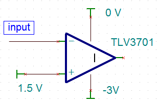
Other Parts Discussed in Thread: TLV3701

Customer would like to use the device SN74LVC1G14 to invert to a negative voltage between 0V and N3V. Input voltage with a mosfet of 0V-P3V3, invert to a negative voltage between 0V and N3V.

And we found a previous post about that, as it said , this is possible. Now customer want to have some simulation and explanation on how this could work.

  • A logic gate outputs voltages at its own power rails. So if you want to output 2 V and −2 V, you have to connect VCC and GND of the logic gate to those voltage. (The trick is that the GND of the logic gate is not the GND of the entire circuit. From the point of view of the SN74LVC1G14, its own power supply is 4 V.)

    The MOSFET circuit generates a voltage of either 3.3 V or −2 V. LVC inputs are overvoltage tolerant, so the 3.3 V input is clamped and output as 2 V.


    Anyway, there is a simpler circuit to do this, with a comparator whose input common-mode range exceeds its rails, such as the TLV3701:

  • Looking further into this solution, the rise/fall times are very slow, are there any IC’s that have a rise/fall time of 5ns or less?


    Also, using the MOSFET and SN74LVC1G14DCK, I don’t want to output +/-2V, I want to output 0V/-3V.

    Please can you confirm that I can connect VCC to 0V and GND to N3V at the IC would operate as required?

  • Hello,

    are there any IC’s that have a rise/fall time of 5ns or less?

    The SN74LVC1G14 will produce very fast edges at the output, typically under 5ns for a light load (15pF).

    Also, using the MOSFET and SN74LVC1G14DCK, I don’t want to output +/-2V, I want to output 0V/-3V.

    Please can you confirm that I can connect VCC to 0V and GND to N3V at the IC would operate as required?

    Yes, the voltage difference from the VCC pin to the GND must be a positive value, so using 0V as VCC and -3V as ground will result in the device operating with the 3V specifications.

    Remember that all voltages are relative -- in a circuit, ground is an arbitrary reference point -- you could place ground at the positive supply of your device and read everything as negative values, although it would be confusing for most people.

    In this case, note that the datasheet values are all written assuming a 0V ground, so you must adjust for your application.

    For example, VOH of the device at 3V supply is 2.4V for a 16mA load. In your case, this would be adjusted by removing the ground offset, so VOH = 2.4 - 3 = -0.6V.

    Similarly, VOL would be shifted down as well. The datasheet lists VOL = 0.4V for a 16mA load at 3V supply, however for your case it would be VOL = 0.4 - 3 = -2.6V