This thread has been locked.

If you have a related question, please click the "Ask a related question" button in the top right corner. The newly created question will be automatically linked to this question.

LSF0102: Schematic design review and VOL confirm

Part Number: LSF0102

Hi Expert,

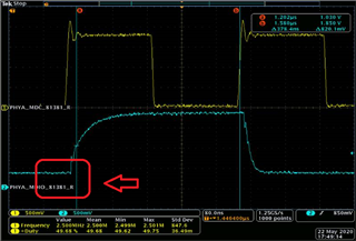
Pls help to review the LSF0102 design and waveform.

Support need

1.Schematic review:

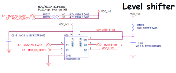
Comment of why the low voltage level on B1 side.

Thanks

Best regards,

Eric Lai


Field Application Engineer

Texas Instruments Taiwan Limited

O: +886-2-2175-2582

M: +886-909-262-582

E-Mail:Eric.Lai @ti.com

  • Hi Eric,

    The low output voltage of an LSF translator will be a combination of the input low voltage to the LSF0102 and the voltage drop across the device due to the current sinking through it. This is explained in detail in this video: Up Translation with the LSF Family 

    Most likely, the customer has a relatively low pull-up resistor value that is causing a large amount of current to sink through the device. The pull-up can be increased to reduce the current, but this will also slow down the signal's rising edge, which seems to be pretty fast currently. I expect that they could get away with about double the resistance while still maintaining the shown data rate without any problems, which should cut the VOL value down significantly (by about half).

  • Hi Emrys,

    Thanks. There is one more item need your support.

    This design Vref_A is 1.2V and Vref_B is 1.8V.

    May we know whether this condition violate the datasheet Table 9-2. Application Operating Condition ? 

    Thanks

    Eric Lai

  • Hi Eric,

    There needs to be at least a 0.8V difference between the supply pins for the bias circuit to operate correctly.

    If a larger supply (for example 2.5V or 3.3V) is available in the system the 200k bias resistor can be connected to that supply instead while keeping the operation of the device the same.

  • Hi Emrys,

    Are you point out the Vref_A is 1.2V and Vref_B is 1.8V is violated the datasheet Table 9-2.

    But why the datasheet saying allow the 1.2 V to 1.8V translation on page 1.

    It confused us between page 1 and Table 9-2.

    Thanks

    Eric Lai 

  • Hi Eric,

    The device can translate from 1.2 to 1.8V, however this requires either a single supply configuration (as described here) or a higher supply voltage for VB. There must be 0.8V minimum between the supplies to produce the correct bias as described here.

    Table 9-2 is an application table - it provides some details regarding the described application of the device. It is not a specification table.