This thread has been locked.

If you have a related question, please click the "Ask a related question" button in the top right corner. The newly created question will be automatically linked to this question.

SN74HCS08-Q1: UNLIMITED input transient rise or fall rate: What does it mean

Part Number: SN74HCS08-Q1

Hello Team, Good Day.

When I gone through the specifications of SN74HCS08-Q1, the value of Input transition rise and fall rate is mentioned as 'Unlimited' nS/V. Does it mean that IC is capable of handling any transition rate? say for example 100V/nS? Its bit confusing. If some numerical value is provided (say 83nS/V), I can understand that maximum allowable voltage rise/ fall in 83nS is one volt. But how to understand UNLIMITED ns/V? Can you please clarify?

Thanks in advance.

  • (2) Will the IC consume any additional supply current when inputs are driven?

    (3) In Datasheet, Pg No 7, in Fig 7.1, what is the value of CL? is it 50pF excluding probe and test-fixture capacitances?

    (4) What is the maximum power dissipation allowed in the package? 

  • Hello,

    When I gone through the specifications of SN74HCS08-Q1, the value of Input transition rise and fall rate is mentioned as 'Unlimited' nS/V. Does it mean that IC is capable of handling any transition rate? say for example 100V/nS? Its bit confusing. If some numerical value is provided (say 83nS/V), I can understand that maximum allowable voltage rise/ fall in 83nS is one volt. But how to understand UNLIMITED ns/V? Can you please clarify?

    Unlimited indicates that there is no limit for that specification. The value can be anything from 0 ns/V to infinity ns/V. In many datasheets, the specification is just left out entirely. We felt including it may help some customers that are unfamiliar with Schmitt-trigger inputs.

    The Schmitt-trigger inputs don't have the same limitations as standard CMOS inputs.

    If you'd like to see more about ST inputs, I have a video explaining them in great detail located here: Schmitt-trigger CMOS inputs 

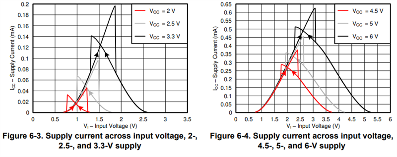
    (2) Will the IC consume any additional supply current when inputs are driven?

    Yes, please see the plots provided in the typical characteristics section of the datasheet. These plots show the expected additional current at the supply pin based on the input voltage. Note that these plots have hysteresis, so the history of the input voltage is important -- the arrows indicate the transition direction for that curve.

    (3) In Datasheet, Pg No 7, in Fig 7.1, what is the value of CL? is it 50pF excluding probe and test-fixture capacitances?

    There is an error in the datasheet -- the Switching Characteristics table _should_ include the load capacitance in the notes at the top of the table, but it does not.

    The correct value is CL = 50 pF.

    I will mark this as something that needs correction.

    (4) What is the maximum power dissipation allowed in the package? 

    [FAQ] Where do I find maximum power dissipation for a device?