Other Parts Discussed in Thread: SN74LVC1G240, , SN74LVC2G241, SN74LXC1T45
Dear TI support team,
I am struggling with a very strange problem. I would like to have a 3.3 V MCU communicate on a 5V SDI-12 bus (cf. https://sdi-12.org/) using one GPIO for bi-directional communication and one GPIO for direction control.
I saw a circuit example (www.daycounter.com/.../SDI-12-Interface.phtml) in which a SN74LVC1G240 is used for this purpose. I tested the adapter device they are talking in the blog post, It is in fact using the SN74LVC1G240 and it works... Only that this circuit requires two GPIOs for communication and one for direction control.
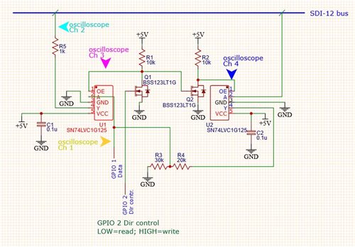
I would like to use only one GPIO for the single-line, bi-directional SDI-12 communication and one additional GPIO for direction control, i.e. setting an alternate z-state of two 3-state buffers (TX buffer and RX buffer). Also I have the inverting logic of the SDI-12 communication implemented software-wise so I decided for the non-inverting SN74LVC1G125.
I also know that effectively the SN74LVC1G125 requires 0.7*VCC for HI on input pins and for a VCC of 5V this would be 3.5V and hence higher than 3.3 V, but this could be solved in one or another way and is actually not my most challanging problem for now...
My problem at this moment is that in my tests it appears that the SN74LVC1G125 I tested are not working properly. Or even worse, sometimes they work some time as expected and then start to malfunction and put out some noisy voltage even in Z-state or also when A is low. Also it appears that, when malfunctioning, there occurs some significant current flow through the OE pin, affecting voltage applied to this pin...
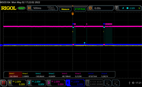
Output of test circuit, here still without buffer connected:
1) OE signal from MUC for TX buffer (pink), data line directly from MUC GPIO without buffer (yellow), inverted OE signal from MUC for RX buffer (turquoise graph, RX buffer not connected in this circuit)
2) OE signal from MUC for TX buffer (pink), data line from MUC via TX buffer VCC 5V (yellow), inverted OE signal from MUC for RX buffer (turquoise graph, RX buffer not connected in this circuit)
-> Even voltage on OE pin becomes noisy and is drifting strongly!
Removing the SN74LVC1G125 from the circuit, everything is back to normal...
Later I found that for the SN74LVC1G125 and I think this is true for all SN74*** buffers, a reflow temp of max. 260°C for < 10 sec is specified and that there is a ESD caution in the spec sheet. While I have to admit that I did not consider these specs in my first attempts, where I hand soldered the SOT23-5 ICs with over 260°C on adapter breakout boards, I am now using low temperature solder, a reflow plate and ESD-protective tweezers and gloves, taking care not to touch the pins of the IC. As soldering below 250°C on the plate did not help I thought that perhaps the temperature ramp of the plate is too flat and duration of the high temperatures too long, still damaging the ICs. To rule out that, I am now even using Fields metal as an Indium based eutectic alloy with a melting temperature of only around 62°C excluding any possible temperature damage… Still the same problem. Many buffers malfunction right from the beginning, some of them after a while with VCC at 5 V.
The best run I had actually was with two SN74LVC1G125s I soldered already more carefully than in the beginning, but still with around 230°C on the plate and tested them in this circuit:

In this circuit I use two SN74LVC1G125, one for TX and one for RX connected to the same GPIO for communication and the OE inputs connected to some inverting mosfet circuit to use one single GPIO to alternate z-State of both buffers simultaneously... I know that I could use the RX SN74LVC1G125 with 3.3 V VCC also for down-translation and would not need the voltage divider. The reason I designed the circuit this way was just the desperate intent to rule out any harming effect of 5 V on A of the RX buffer, although according to the spec sheet this should be no problem anyway...... Now I also found the SN74LVC2G241 which is actually including all the features of my designed circuit and I will also test it...
The results of this test circuit, oscilloscope graphs and comments below, see below...
It is to say that I had these strange failures with more than 20 SN74LVC1G125 units I soldered on SOT23 adapter boards.
In some cases I get a wrong and drifting voltage on Y immediately although A is low and OE is high and in some cases it works some time before Y is driven up and noisy...
Now, as I am using a low temperature solder and even an eutectic alloy with melting temperature way below the specified normal operation temperature maximum of the SN74LVC1G125 and furthermore ESD-safe tweezers and gloves, I remain just puzzled what could still be the issue.
What am I doing wrong? Furthermore, it is to say that I ordered the SN74LVC1G125 from a well-known and large german parts reseller with good reputation and I would actually not expect any problems with fake chips or inproper handling there. The SN74LVC1G125 came in the original reel-tape but packed in, as far as I can see, normal plastic zip bags. No ESD-save bags... but could it really be that the ICs are so delicate to handle...?
Any help and suggestions are highly appreciated...
Best Michael
Test data of the above circuit:
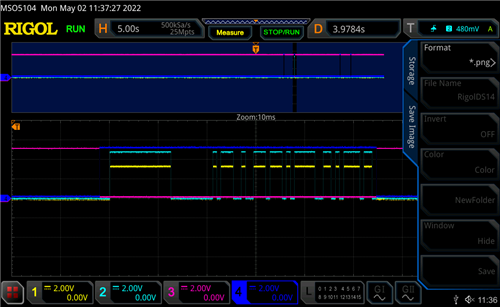
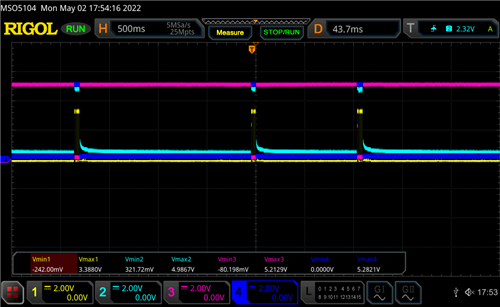
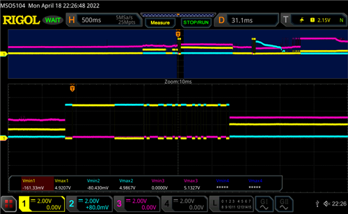
1) Just testing TX buffer with RX buffer not connected yet:
OE level on TX buffer is HIGH by default (pink graph), and OE of RX (here not connected yet) is LOW (blue graph)-> i.e. listening state
For writing the SDI-12 bus the state of the OE pins of both buffers is alternated and the MUC writes (yellow graph) the writes the SDI-12 bus via the TX buffer (turquoise graph). After writing it returns to listening.

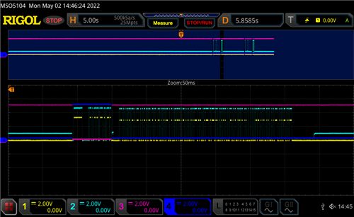
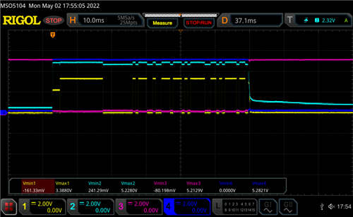
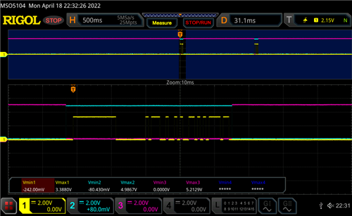
2) Now testing SDI-12 communication with both buffers and a SDI-12 sensor connected to the bus. The MUX switches buffer states to writing state where OE of TX buffer is LOW (pink) and OE of RX is HIGH (blue) and the data GPIO writes the request with 3.3V (yellow graph) via the TX buffer to the SDI-12 bus with 5 V (turquoise graph). After writing request the MUC resets OE states again to listening (pink is HIGH, blue is LOW). The connected SDI-12 sensor replies at 5 V level on the SDI-12 bus (turquoise grap) and the RX buffer receives the signal on the SDI-12 bus and via the voltage divider the sensor's reply is received on 3.3 level on the data GPIO (yellow). Well great, so far It works...!

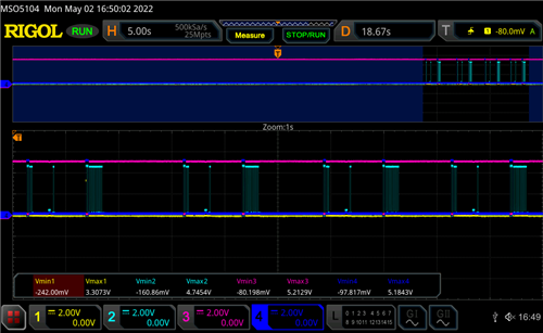
3) And after some time with the whole circuit powered-up it still works. I have no screen shots of the oscilloscope here, but communication still worked the same way after some 20 minutes having with the whole circuit powered-up and the MUC circuit in "listening" state.

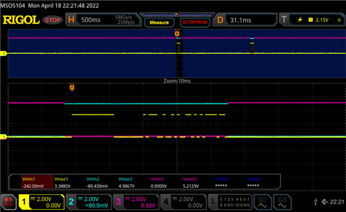
4) But then without doing any changes... again the ICs start to malfunction... First the level on the mosfets switches change voltage level and get noisy

5) And then also the buffer output starts to deliver outputs where it shouldn be

6) This is where the buffers stop to work completely...