This thread has been locked.

If you have a related question, please click the "Ask a related question" button in the top right corner. The newly created question will be automatically linked to this question.

SN74GTL2003: SN74GTL2003

Part Number: SN74GTL2003
Other Parts Discussed in Thread: LSF0108,

HI 

Please help me understand with below queries about pass transistor based level translators

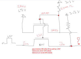
1) How do these pass transistor-based level translators work without any pullup resistors on Dn and Sn sides?

2) Are there any internal pull-up resistors on Dn and Sn sides?

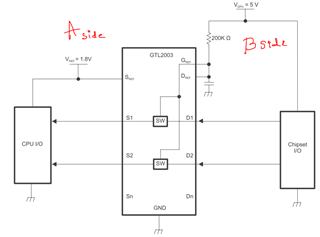
3) What is the purpose of the Reference pass transistor? are all the Sn pins of different channels connected to SREF and Dn pins connected to DREF internally?

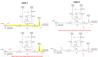
4) how does the down translation from Dn(B-side) to Sn(A-side) work? if B-side is at 5V and the A-side is 3V how does logic 1 on B-side translate to Logic one on A-side?

5) which side is Source and which side is Drain between Sn(A-side) and Dn(B-side)? what are the turn-on and turn-off conditions for these pass transistors?

Thanks

Santosh

  • The SN74GTL2003 is pretty much identical with the LSF0108. See [FAQ] How do the LSF translators work?

    1) In general, without any pull-up resistors, they do not work.

    2) No.

    3) Only the gates are connected together. The GREF/DREF/200 kΩ circuit ensures that the gate voltage is above SREF by the transistors' threshold voltage. This means that for all voltages between GND and SREF, the transistors are closed, while for voltages above SREF, the transistors are open.

    4) The B side cannot pull the voltage at the S pin higher than SREF because the transistor would open.

    5) The sides are labelled "S" and "D", but the transistors actually are completely symmetrical. The characteristics of the pass transistors are not specified; the GREF circuit uses negative feedback to bias the gates to the desired voltage.

  • How does it work with only one Pullup resistor on Dn side and no pullup at Sn aside at all (i have a working board with just one pull up on Dn side and no pull up on Sn side)?

    If I tie SREF to 1.5V and DREF and GREF to 3.3V then the pass transistor is always on right? considering the signals on Sn side are togelling between 0 and 1.5V

  • See section 5 of the application  note linked to from the FAQ.

  • which application note should I refer to? where is it attached?

  • See the link in my first answer.

  • above is the screenshot from the application note.

    CASE1: When the signal is flowing from A-side to B-side I could draw the flow as seen in the image(yellow highlight)

    CASE2: I am not able to understand what is the flow when the signal flows from B-side to A-side. in what condition pass transistor is ON and what condition it is off from B-side to A-side? Please clarify

    For both cases, consider A-side is 1.8V and B-side is 3.3V

  • The EN/Vref_B/200 kΩ circuit regulates the gate-to-source voltage (EN to Vref_A) so that this is the voltage where the transistor allows only a very small current to pass (it's partially open).

    When the B side is 0 V, the transistor is closed, so the A side is connected to 0 V.

    When the B side goes to 3.3 V, the voltage on the A side rises until it reaches about 1.8 V. It cannot go higher because then the transistor would close completely.

    This is a clever circuit, but a pull-up resistor on the A side would make the circuit faster and more robust.

  • "When the B side goes to 3.3 V, the voltage on the A-side rises until it reaches about 1.8 V"

    what happens when A side rises to 1.8V and then after that how does the Pass transistor turn off itself? what is the turn-off condition immediately after the B-side input reaches 1.8V?

    For the pass transistor to turn off VG should be less than VT right? Which is the gate terminal which is Source and Drain terminal in this case?

  • The pass transistor turns almost off because the gate-to-source voltage becomes small enough. This is the same state that the reference transitor is in; all gates are connected to EN.

    The body of the transistor is not connected to either side (but to GND), so you can call the A/B pin with the lower voltage the source.