This thread has been locked.

If you have a related question, please click the "Ask a related question" button in the top right corner. The newly created question will be automatically linked to this question.

SN74LVC2G126: Output Rise/Fall Times

Part Number: SN74LVC2G126
Other Parts Discussed in Thread: SN74AUC2G126, SN74AUC1G126

With VDD = 1.8V± 5%, can this device support 66.66MHz input square wave?

What is the expected Tr/Tf for CL = 15pF in this case?

Has this device been observed to be used in applications that buffer a clock signal?
(I worry about jitter and clock signal degradation...)

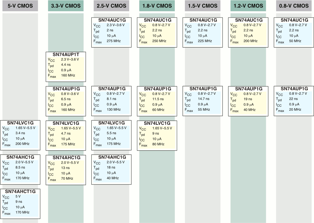
  • At 1.8 V, LVS can do 80 MHz.

    See [FAQ] What is the output transition rate for a logic device?

    At 1.8 V, AUC family devices like the SN74AUC2G126 work much better than LVC. (Please note that AUC outputs change impedance during transitions, so the rise/fall time cannot be easily estimated as in the FAQ; see the AUC application report.)

  • Hi Darren,

    We don't specify jitter for standard logic buffers -- for this type of specification, you will have to switch to a clock buffer.

    I agree with Clemens -- while the LVC can handle 66.66MHz, I would not recommend it as my first solution. The AUC family is much better at 1.8V.

  • Hi Emrys,

    I still need to know the expected rise/fall times of the output. Do we have any data for the following conditions?
    I need max/min if possible.

    - VCC: 1.8V or 3.3V
    - Tr/Tf Range: 20%~80% VCC
    - Tr/Tf Range: 35%~65% VCC
    - CL: 15pF

    I expect the output Tr/Tf to be independent of the input Tr/Tf, yes?
    (A logic buffer is not an amplifier; output is triggered when input passes a certain threshold)

    Regards,
    Darren

  • Hi Emrys,

    I read through your blog post and did some math.
    I think I have a pretty good understanding of the process (t = -RC*ln(1 - dV))
    Can you check my math (excel)
    I was getting <200ns for LVC at 3.3V and ~300ns for AUC at 1.8V.
    (CL = 15pF and 35%~65%Vcc = dV = 0.3) These numbers use MAX rds(on) so are really kind of worst-case?

    Would the AUC logic buffer SN74AUC1G126 be able to handle 125MHz input/output?
    It is a 4ns/4ns H/L signal, and I'm a little nervous about the 1.4ns max tpd.

    Any logic device you would recommend for 2.5V / 125MHz?

    Regards,
    Darren

  • That calculation does not apply to AUC outputs; see the AUC application report.

    Why do you care about the rise/fall time? If the propagation delay is smaller than the period, it will definitely work.

    AUC also works at 2.5 V.

  • Hey Darren,

    With a typical load, the rise time for an AUC device will be under 1ns. These are the fastest devices in the logic portfolio.

    Do we have any data for the following conditions?

    No, I'm afraid not. Rise and fall times were not part of the specification or characterization of the device -- if they were, they would be in the datasheet.

    I expect the output Tr/Tf to be independent of the input Tr/Tf, yes?
    (A logic buffer is not an amplifier; output is triggered when input passes a certain threshold)

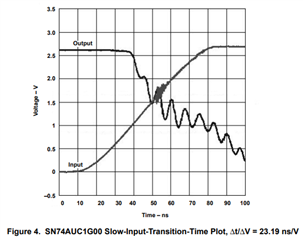
    Yes, this is true, however a slow input can cause erratic behavior which will affect the output signal. All CMOS inputs need to meet the datasheet requirements:

    From the application report Application of the Texas Instruments AUC Sub-1-V Little Logic Devices 

    I read through your blog post and did some math.
    I think I have a pretty good understanding of the process (t = -RC*ln(1 - dV))
    Can you check my math (excel)
    I was getting <200ns for LVC at 3.3V and ~300ns for AUC at 1.8V.
    (CL = 15pF and 35%~65%Vcc = dV = 0.3) These numbers use MAX rds(on) so are really kind of worst-case?

    I think you're off by a factor of 1000 (I did not check your excel). For 10% to 90%, you can use the easy equation: t_t = 2.2 * R * C

    With CL = 15pF and an LVC device (about 13 ohms), the rise time is calculated as  approximately195 ps.

    As Clemens mentioned, the AUC device has a variable output impedance, so this type of calculation won't work very well with it.

    -

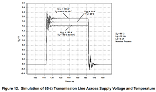
    From the same application report I linked earlier, there's a waveform for driving a transmission line from an AUC family device at 1.8V:

    As you can see, the edges are extremely fast. The AUC family easily drives 125 MHz signals.

  • Hi Clemens,
    I appreciate the comments. We care about Tr/Tf as there are pretty strict requirements for the receiving device.
    (i.e. 513ps max rise time for 15pF load, measured from 35%~65% of the signal amplitude)

    Hi Emrys,
    You're right, I meant to say [ps] not [ns].

    Figure #13 of that document you attached made it much easier to see the typical Tr/Tf for 5pF.
    Definitely below 1ns...

    Last question:
    I noticed the datasheet specifies "tpd" as a stand-alone value.
    Does this mean tpd for H-L transition and L-H transition are exactly the same?
    If there is skew, how much? This information is important to understand how much duty-cycle degradation to expect at the higher frequencies.

    Regards,
    Darren

  • If you have calculated 0.3 ns with the DC resistance, then the actual rise/fall time (where the output impedance is much lower) will certainly be below your limit.

    CMOS devices are designed to have symmetrical outputs. But the remaining skew is neither specified nor guaranteed.

  • Does this mean tpd for H-L transition and L-H transition are exactly the same?
    If there is skew, how much? This information is important to understand how much duty-cycle degradation to expect at the higher frequencies.

    No, it just means that the larger of the two values will not exceed the limits provided in the datasheet. t_pd is a shorthand for the larger of t_plh and t_phl.

    Skew is not specified.

    I would recommend them to look at TI"s clock buffers portfolio, as those will have jitter and skew specified and have excellent performance.