Other Parts Discussed in Thread: LSF0108,
Hi Ti support team,
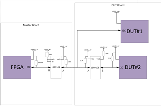
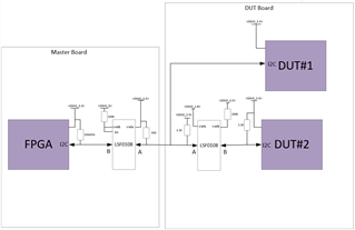
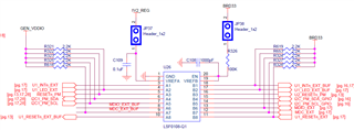
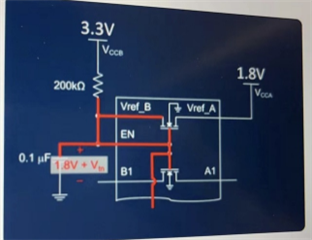
We encountered one issue when using LSF0108-Q1 level shifter. Below is the schematic. We connected VrefA to 1.2V source. VerfB and EN are tied to 3.3V source through one 100 kohms resistor. The signal for A side to B side is ok. But we met issue when translating signal from B side to A side. In our case, A side ports are connected to a FPGA whose VDDIO can be either 1.8V or 2.5V or 3.3V. But B side ports are connected to a fixed 3.3V DUT. For bidirectional pins such as SDA, translation from A side to B side is ok. But when signal direction is reversed, if B side input and high level signal, A side output will be clamped at VrefA which is 1.2V. But we have a pull up the pins to the VDDIO of FPGA. What we expect is that the high level output of A side should depends on the pull-up source. We have watched the video of LSF family level shifter. We think that the A side output high level voltage shouldn't be clamped by VrefA according to the structure of LSF0108 as below picture shown. Do you have any idea about this issue? Thanks!
thanks and best regards,
chaodong