This thread has been locked.

If you have a related question, please click the "Ask a related question" button in the top right corner. The newly created question will be automatically linked to this question.

SN74AUP1G74: More details requested regarding Ioff protection and interplay with ESD diodes during Vcc Ramp up and down

Part Number: SN74AUP1G74
Other Parts Discussed in Thread: SN74AUP1G08

Tool/software:

Hi,

I am working with several TI logic devices that state they support Ioff protection and Partial power down protection. I have searched and read through just about everything I can find online both from TI and other vendors to try and better understand the dynamics of the Ioff protection mechanism.

In particular what happens when an IC like the D-FLOP referenced here has an input pin connected to a low impedance voltage source that can deliver considerable current. Such as a Li-ion cell, and then the Vcc pin is relatively slowly raised from 0 to its working voltage. The specifications for Ioff feature are not entirely clear about the lower threshold on Vcc when Ioff activates. Furthermore there is no information about what happens in the transition region when Ioff is deactivating and the device has not reached its minimum Vcc, still further Even if Vcc has exceeded min Vcc on voltage it may still be at a lower voltage than an I/O pin and we might still see the ESD diodes forward biased. In these conditions we could in fact theoretically see quite a large voltage difference between Vcc and an I/O pin and potentially damaging current.

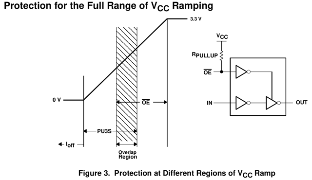
Is this actually true or are there multiple protection taking place that continue to isolate the I/O pins until Vcc exceed the I/O voltages? I see nothing in the datasheet of the DFLOP to suggest this but I have read a application note from TI that discuss PU3S protection. I do not believe the D-FLOP has this mechanism, but interestingly this app note has a somewhat confusing paragraph regarding Ioff. I quote.

"For devices with only an IOFF specification or without any of the IOFF, PU3S, and precharge specifications (for example, LVC and ALVC), GND and VCC need to be powered up to the recommended operating level before output or I/O ports can be exposed to any live signal. A device output or I/O port can be exposed to a live signal with VCC = 0 V if IOFF is specified for that port. But an input port, with IOFF, can handle a live signal when VCC = 0 V and while VCC is ramping up or ramping down. This is why an input port connection can occur any time after the GND connection in the power-up sequence, if that port has IOFF specified."

This suggests that the behaviour of input pins is different to that of output pins, but is this true and does this only apply to the device families mentioned?

I am using other devices that also state they have Ioff protection but again in these cases also, the threshold voltages for protection and the behaviour of the devices in the transition as Vcc ramps up or down and the differences in input versus output pins is not entirely clear.

Could you please help me with a more detailed description of the internal structure of these circuits on which pins it applies and how to read the datasheets to extract any relevant data, then I can decide under which circumstances I need to consider external current limiting. I have read several app notes from TI even ones specifically referencing what information is contained on datasheets in respect to Ioff function, but even these do not clearly answer my questions.

I look forward to some clarity,

All the best.

  • Hi Aidan Walton,

    If a device does not have overvoltage protection, you should avoid scenarios in which Vis greater than Vcc. As you said, this situation may result in a potentially damaging current. I believe you're referring to the presence of a positive clamp diode to "back-power" a device. A great explanation on the changed behavior of a circuit with or without a positive clamp diode can be found Here. Without a positive clamp diode, the risk of back-powering in the manner you describe goes away.

    The specific device you mention (SN74AUP1G74) does indeed have over-voltage tolerant inputs. This means that in addition to IOFF there is no positive clamp diode. Generally speaking, "over-voltage tolerant inputs" is a phrase used that is used to describe when a device will allow Vgreater than Vcc without fear of back-powering.

    Regarding more specifics on the internal structure, please see the below image as an example of how IOFF works. This image was taken from page 42 of TI's Understanding and Interpreting Standard-Logic Datasheets and is an excellent resource. You may also be interested in Section 4.6.12 of this document which describes the II Input Current. It describes how this specification is relevant to devices that have overvoltage-tolerant bus-hold inputs which use Schottky blocking diodes to prevent back-flow of current.

    You had several good questions. I hope I was able to provide some clarity.

    Regards,

    Nikki

  • Thanks for attempting to help further, but I'm afraid to say I had already read these documents and although it seems at first sight like a reasonable explanation. I do not see how the Ioff feature works with this structure. Sure all these diodes are arranged in such a way as to block current flow from a device pin I/O towards Vcc. However what happens with respect to the ESD didoes. As we can see in this diagram there is no diode forward bias path between the I/O and Vcc. Therefore how/where does it exist? If it is switched in and out of circuit by the Ioff feature, then it is not shown in this diagram. Which BTW I have seen repeated over and over in various application notes. 

    If we assume some mechanism for switching the ESD diodes into circuit, when does this occur. Figure 4 of SSZTAP0 application note shows some kind of transition occurring as Vcc rises/falls somewhere around 0.5-0.6V. This is kinda confirmed in several datasheets. Yet other datasheets for other devices show these transition voltages to be around 0.3-0.4V.

    Essentially it is not clear, furthermore, I have found other forum posts that state (TI representative) that there are circumstances where Vcc must be hard clamped below this threshold voltage with a significant pull-down to avoid having the devices floating above these Ioff transition levels.

    It does seem unfortunate that most datasheets do not explicitly state what this voltage level is. Can you explain why this is so?

    Please also review SZZA033 for me. I have attached the diagram regarding Vcc ramping from this application note:

    We can clearly see here what is described as an overlap region. Now this seems to be related to the PU3S feature. Which I think the D-FLOP in question does not support. However my earlier questions still apply. 

    If there is no active mechanism to hold the inputs or outputs in a high Z state while Vcc rises or falls above or below an I/O, then what stops potentially destructive currents from flowing through an ESD diode as soon as it is "switched" into circuit the moment Vcc rises above an I/O pin, and likewise what prevents destructive currents flowing from an I/O pin into Vcc if Vcc is above the Ioff level but below the I/O level.

    It seems this situation is not entirely clear to me and certainly does not seem well defined in any datasheet.

    All the best

  • Hi Aidan,

    I think some of the confusion is with regard to how our ESD diodes work.

    some mechanism for switching the ESD diodes into circuit

    These diodes are not related to the IOFF or turning the device on or off. ESD protection circuits wait to be triggered by an ESD event and are otherwise not used. A good video about ESD protection commonly used in logic devices can be found Here. However, these ESD circuits shouldn't be confused with IOFF or over-voltage tolerant inputs. 

    It does seem unfortunate that most datasheets do not explicitly state what this voltage level is. Can you explain why this is so?

    This has to do with how TI has historically made their datasheets. Up until recently, this specification was only measured at 0V. Newer devices are tested at 0V and 0.3V, so you may find that in new datasheets. Unfortunately, this is the reason why I can't help you define that voltage level for older devices where the voltage level isn't specified. You're right that this number varies, and you're more likely to find 0.5V listed for older devices. If you need a general rule of thumb when the voltage isn't listed, 0.3V is a safe bet.

    Please let me know if I need to clarify further.

    Regards,

    Nikki

  • Thanks Nikki for your response. In terms of the second part I am happy to accept this answer but one of the reasons that I am looking for such detailed information is that my day job is building customised spice models for devices where a manufacturer does not offer a suitable model Instead I derive them from datasheet info and in this case we are attempting to model scenarios where we seem to be back powering through ESD protection didoes. and therefore the specific and accurate voltage levels for Ioff and and transition in or out of this mode and also and interaction with PU3S circuits (which you did not comment on in your review) is very important.

    Still further I am not convinced by your comments about ESD diodes doing nothing until they are triggered. I think you refer here to the reverse breakdown region which is very much the case for bi-directional interfaces. However on digital devices the structure I was expecting to consider is using the forward biased mode. I am very happy to be corrected, but please take a look at the table from TI's own application note: SSZT784 "Reverse Working Voltage , Breakdown Voltage and Polarity Configuration"

    In this case it is clear to my mind that in the case of a digital circuit where the I/O line exceeds the Vcc voltage we will have a forward biased diode in place. This diode would not be operating in Avalanche mode so if it is not to conduct as in the case of Ioff, it must be isolated from the circuit.

    What am I missing?

    Thanks again.

  • Hi Aidan,

    building customised spice models for devices

    Thank you for providing context for your questions. For the initial device you were asking about (SN74AUP1G74),  LTSPICE (and similar) does not support digital circuits that include latches such as flip-flops. These circuits can produce unknown states and cause convergence errors in the simulator. Forgive me if you're already aware of this and are using a simulation tool for which this does not apply.

    However, for most of our devices we provide SPICE models in the Design & Development sections of our product pages. For example, if you were interested in the SN74AUP1G08 (a device that has over-voltage tolerant inputs and partial power down (IOFF) features), you could go to SN74AUP1G08 Design & Development and download a SPICE model that we have created. We believe is a good representation of our part. You're also welcome to edit or use the information provided in our SPICE model to assist in making your own model.

    attempting to model scenarios where we seem to be back powering through ESD protection didoes

    Beyond the recommended / absolute maximum datasheet parameters, the device is likely to be damaged. Therefore we don't include any out-of-spec behaviors in our model. However, I understand now that you're making your own model.

    I am not convinced by your comments about ESD diodes doing nothing until they are triggered

    You are correct. I apologize for any confusion I've caused on the matter. I didn't mean to imply that they do literally nothing. Parameters such as leakage current, for example, are listed in our datasheets.

    the specific and accurate voltage levels for Ioff and and transition in or out of this mode and also and interaction with PU3S circuits (which you did not comment on in your review) is very important

    As mentioned, the specific voltage levels are something we not have historically tested, so besides 0.3V testing for recent devices, I'm afraid I cannot give you any details. I also cannot provide data about its interaction with PU3S circuits. If you're asking for specifics about the internal circuit, I'm afraid I cannot provide that because it is proprietary.

    In this case it is clear to my mind that in the case of a digital circuit where the I/O line exceeds the Vcc voltage we will have a forward biased diode in place. This diode would not be operating in Avalanche mode so if it is not to conduct as in the case of Ioff, it must be isolated from the circuit.

    What am I missing?

    I believe you may be looking for information that I cannot provide. Specific circuit details and exact schematics for the internals of our parts are proprietary. However, you're more than welcome to edit or do whatever you see fit with the SPICE models we provide on our product pages. If the SPICE models are not enough for your needs, the best way to find answers may be to bench test our devices on your own.

    If you have questions about a specific device, I can attempt to seek answers for you. I think some of our miscommunication has come from speaking generally about protection circuits rather than about specific devices.

    Regards,

    Nikki