This thread has been locked.

If you have a related question, please click the "Ask a related question" button in the top right corner. The newly created question will be automatically linked to this question.

SN74HC109 alternatives

Other Parts Discussed in Thread: SN74LVC1G74, SN74LVC2G132

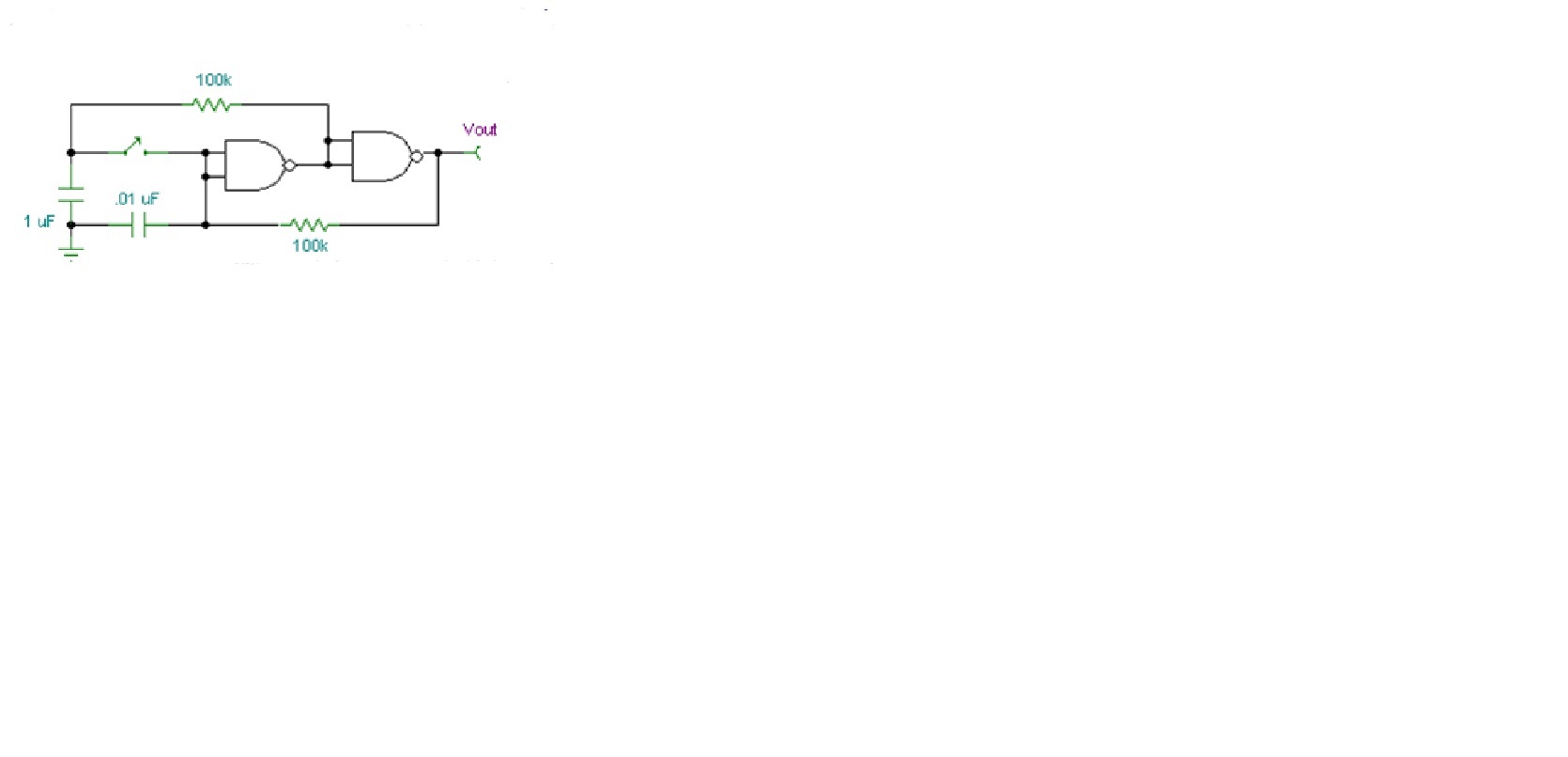
All I need is a basic toggle function for controlling the enable pin on a multiplexer.

I want this to be a push button application so I need proper debouncing, specifically a schmitt trigger.

Are there any j-k flip flops or toggle chips with built in schmitt trigger?

  • Hi,

    I have installed the same circuit and it works BUT it is very sensible.

    Have you got any suggestion on passive components values about my issue ?

    BR

    Theodore Belogiannis

  • Theodore,
    Can you post a schematic of your current circuit and/or scope shots of what you mean by 'sensible?'
  • The schematic is like yours with SN74LVC2G132DCTR , Vcc 4.5V (3xAAbatteries) , instead of 1μ I use 0.1μF, toggle switch is a reed (with magnet) switch, I drive a shutdown pin of an 3.3V LDO. Circuit is activated (i.e shuts down the LDO) during operation without reason...
  • Can you post scope shots of the input and output signals?
  • Hi,
    Unfortunately no(I have an analogue scope without recording) . But toggle operation works fine. I just dont understand why after some time (hour or more) the circuit is activated.
    It might be that LDO is shutting down but also there is no reason for this.
    Thats why I'm wondering about the toggle circuit.
    Is the 0.1μ instead of the 1μF capacitor of great importance ?

    BR
    Theodore
  • Theodore,

    Before I get into my answer, can you replace this circuit with something made for this application, such as a flip-flop (ex: SN74LVC1G74 )?  Having a circuit that is designed bistable would be far superior to this setup.

    The short answer is that the smaller capacitor will reduce the stable time of the system by about 13.6%, which is probably not enough to cause any major issues.  How I arrived at this follows:

    When the switch is closed, the two capacitors are placed in parallel and thus the charge on them is shared.  The equation governing this is Q = C*V.

    For example, if the 0.01 uF cap is discharged (0 V), then the output of the first inverter stage will be high and the 1 uF cap will be charged to 5 V by the output of the SN74LVC2G132.  This puts Q1 = 0 C and Q2 = 5*1 uF = 5 uC of charge in the system (Q = Q1 + Q2).

    When the switch is pressed and the two capacitors are placed in parallel, 5 uCoul = V(C1 + C2) yields a final voltage of  5/1.01 V = 4.95 V on both capacitors -- which means the 0.01 uF capacitor has 4.95 * 0.01 uF = 49.5 nCoul of charge on it when the button is released.

    If the 1 uF capacitor is replaced with one 10 times smaller (0.1 uF), then the final charge on the 0.01 uF capacitor will be reduced to 45.5 nCoul (using the same process as above to solve).

    The leakage current into the chip will cause the capacitor to discharge over time, which will eventually cause the system to switch without any user input (when the capacitor discharges to ~2 V).  Since current is simply change in charge over time, the system with more charge will remain above 2 V longer.

    The charge at 2 V on the 0.01 uF capacitor will be 20 nCoul, so the final difference in discharge time (assuming constant leakage current) will be (49.5-45.5)/(49.5-20) ~= 13.6%

  • Thanks a lot for your analysis!

    It has definitely much sense to try the D-flip flop but pcb's has been made and assembled. The pins are somehow compatible but it will need much rework on the pcb which is not so good.

    On the other hand you showed me that bigger capacitor wont improve discharge time much.

    It looks like a deadlock.

    Any suggestion from the experts ?

    BR

    Theodore


  • You might be in luck.  It looks like the flip-flop I suggested comes in the same package and has a very similar pinout.  I will take a look and see if there is a way we could modify your design to accept the flip-flop without making a new board.  If that fails, I'll take a second look at the original design to see if a component change might help.

    To make sure I understand the design -- is the output taken from pin 3 or 7 of the SN74LVC2G132? I don't see how this interacts with the rest of your system.

  • I noticed a discrepancy between your schematic and the original post by Chris.  R4 is connected in the wrong spot.  Below you will see Chris's original circuit, then your original, and my suggested fix.  I'm not really sure how you might be able to pull this off without changing the board though.  Since it's just repositioning a resistor, you might be able to do it with minimal modification.


  • Hi,

    I really appreciate your help.

    Pin 3 is the output.

    This is how the board has been made. At the 2 holes is the reed switch and far right is the pin it toggles.

    BR

    Theodore

  • Theodore,

    I believe two relatively easy changes could fix the trouble you are having.  The green line I added indicates a trace cut, the blue line indicates a wire connection.  All of the components should remain the same.

  • Hi,

    You really saved me. I have already start modifying the boards. (50pcs)

    I don't know how I did such a mistake. The old circuit was somehow working though but with so many problems.

    I really appreciate your help.

    BR

    Theodore