This thread has been locked.

If you have a related question, please click the "Ask a related question" button in the top right corner. The newly created question will be automatically linked to this question.

74LV counter using as prescaler

Other Parts Discussed in Thread: MSP430F435

Dear All,

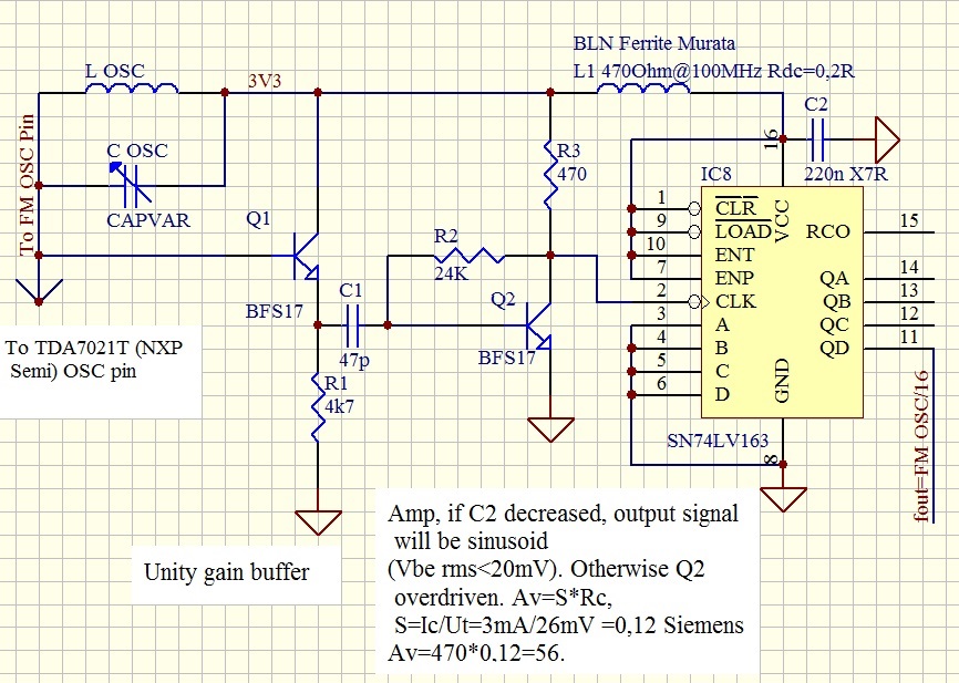
I would like to use a 74LV163AD 4-bit counter as precaler (1/16) applied to FM radio receiver oscillator (fosc=100MHz). Supply volatge is 3V3.

The oscillator level is ca 240mV RMS. Prior to the '163 there would be a two-stage RF amp to increase level to

 ca 1-2Vp-p using BFS17 transistors (first in common collector secod in common emitter operation). Unfortunately OSC level cannot be so high to avoid radiation. The '163 CLK

input would directly connected to the out of RF amplifier which is biased to VCC/2.

I would like to ask wheter you have any experiments about similar applications when "standard" logic family is used instead of dedicated

prescaler circuits?

Many thanks for the comments in advance!

  • Joseph,
    This sounds like an interesting application. The forum post I found below talks about using standard logic devices in an FM receiver.
    http://e2e.ti.com/support/logic/f/151/p/347707/1217788#1217788
    If that post does not help answer your question, could you please attach a block diagram or schematic in your response? That will help me find a solution.
    James
  • Dear James,

    thanks for the response! I would like to measure FM oscillator frequency.

    I attach the schematic. The LV163 would be fed from the Q2 transistor (DC coupling), whose collector voltage biased (by trimming R2) to VCC/2 (CMOS threshold).

    What do you think, LV163 would correctly operate if input signal not an ideal square wave but an amplified RF signal? I do not want to use extra added Schmitt trigger (LVC1G14) because it might increase the EMI problems (Radiation of OSC signal) and consume more place and current...

    The internal inverter of LV163 at the CLK pin may can form the input signal to a useful square wave for other parts of inner logic.

    Thanks and regards,

    József

  • Here are the care about in this circuit.

    1. The rise and fall time on the clock with Vcc at 3.3V should be faster than 100ns/V.  You can take a measurement to confirm this. Slower than this could cause double clocking.

    2 The Vih and vil on the input  must also be observed .3 x Vcc for ViL and .7 X Vcc for Vih. Looking at the schematic you are probably Ok here.

  • Hi Chris,

    Thanks for the remarks!

    unfortunately, I cannot make any measurments, because this circuit is only an idea, I do not have neither 74LV163 nor a trial PCB.

    That's why I wanted to ask the Forum before ordering (unfortunately 74LV163 is not available in the local electronic components shop in my city..) parts and make PCB to check wheter there is any chance to operate:)

    About rise and fall times:

    The freqnecy range 88..108MHz, ->the periode: ca 10nsec. So, the tr, tf<periode time/4, 2,5nsec. But, It should be noted at Q2 collector

    the rise time higher (Q2 turns off) and fall time lower (Q2 turns ON) assuming Q2 is overdriven.

    Therefore there will be a signal fot LV163 with tr=3..5nsec and tf=2 nsec, frequency 100MHz (tcyc=10nsec) and peak levels meet with logic levels spec as you mentioned.

    Yes, it might be a critical application for LV163 device but i hope Its performance still enough for this job.

  • I ran a Spice simulation of your amplifier and I have two comments:
    1) If the drop across L OSC is very small, then Q1 will be operating at or close to saturation and won't work well. In that case you need to cap couple into Q1 and add a bias network. The SPICE simulation showed good operation at or below a Q1 base DC operation point of 3.0V with a supply of 3.3V. If you want to play around with the circuit in simulation you can download LTspice for free and get the BFS17 model from the NXP site. I found that for an input amplitude of 25 mV I needed to reduce the value of R1 to about 1.2K and I also needed to change R2 to 20K to get a centered voltage swing of about 1.0V to 2.3V into the clock pin.
    2) The 74LV163A is not guaranteed to run at 100 MHz. The typical spec is up to 160 MHz, but if you're planning to build more than one of these you should probably look for a higher performance logic family.
  • Dear Gabor,

    thanks for the remarks!

    You have right referring to Q1 buffer, its colletor-base voltage might be below 0V. Not so elegant solution, however, diode will not open (but capacitance feedback insreases somewheat) because osc signal <250mV.

    Similar buffer used in the TDA7030T IC datasheet (Micro Tuning System for Tda7021T radio, my application replaces/emulates the 7030T using a TI MSP430F435 MCU) application section for interfacing to 7021T. It is interesting to note the TDA7030T appeared first in the 1992 Philips Data Handbook IC01 (ICs for Radio and Audio systems) and it any more mentioned in the 1997 Edition, despite its pair, the 7021T was still in production almost for two decades)

    I order 74LV163 to try. The circit will not be in mass production, I undersand why you pointed to this topic.

    I do not want to use faster logic than minimum expected (even if ONLY its TYPICAL speed parameter meets the requirments) because of the sensitivity issues to

    rise/fall times, increased power consumptions and possible EMI problems.

    Reading the answers in the forum, the circuit has a chance to operate on such high frequency (Nobody states that LV163 will not operate properly)

    I will come back with the experiments.

  • Hi,

    the 74LV163s arrived, I tried the schematic. It worked properly at first, no additional tuning was required!

    At 100MHz, (VCC=3,2V) there was a nice (stable) signal at the LV163 output, there was not any jitter etc watching on scope.

    The output square signal (a Q0..Q3) periode is chaning by varying the capacitor of 7021 oscillator.

    at 100MHz, LV163 current consuption ca 10-11mA, quite low on such high freqency!

    I could not check input signal very well because the min time base on my scope only 50nsec (there were 5 peak in a DIV).

    Using the probe in 1/10 (decrease the capacitive load) mode the peak to peak was ca 1V at Q2 output.

    I really like the 74LV163, it is an amazing product!

  • That's great.

    The resistor changes I noted were necessary when I ran the SPICE simulation with only 25mV amplitude on the input sine wave.  I wasn't sure of the actual swing on the input voltage in your circuit, so if it is significantly more than 25mV it's not surprising that the circuit works as originally designed.  One thing I noted in the simulation was that the output was not very symmetric without the changes.  Given the spec for high and low time of the 74LV163 I was concerned that you needed fairly close to 50% duty cycle to meet the spec.  However it seems that's not a problem when the part is operating at its typical rather than worst case ratings.

    It sounds like you could use a better oscilloscope.  It's likely that the Q2 output is swinging more than the 1V p-p you measured, but the probe or scope bandwidth attenuates the signal.  If the signal looks sinusoidal on the scope it's also likely that the scope's bandwidth is blocking out most or all of the harmonics.  In any case if the circuit is properly clocking the 74LV163 it doesn't really matter.

  • I have not used 74 series logics at such high frequencies prior to this app, so, I was supprised it is working reliable. Its really great, when the preditions (and theory)

    successfully validated by the practice.

    This experiment showed the frequency domain previously dominated by ECL, by todays, has been an applicaton area for 74 series of logic family.

    My impression is that, the ICs generally are better than their specs (not only this LV163):)

    Yes, the waveform was sinusoid at Q2 due to harmonic suppression by not only the scope cable, but due to prasitic load capacitances as well, around the collector resistance.

    The signal is not even square wave if no loading calble (due to on board/chip load capacitances), as the simualtion showed.

    However, LVC series might cause jitters because it specified for stricter rise, fall times. I do not know, but I think the LV is ideal for this app (up to 110..120MHz).