This thread has been locked.

If you have a related question, please click the "Ask a related question" button in the top right corner. The newly created question will be automatically linked to this question.

Sharing the XINTF on F28335

Other Parts Discussed in Thread: SN74LVC1G19, SN74LVC1G3157, TS5A23157-Q1

Hi

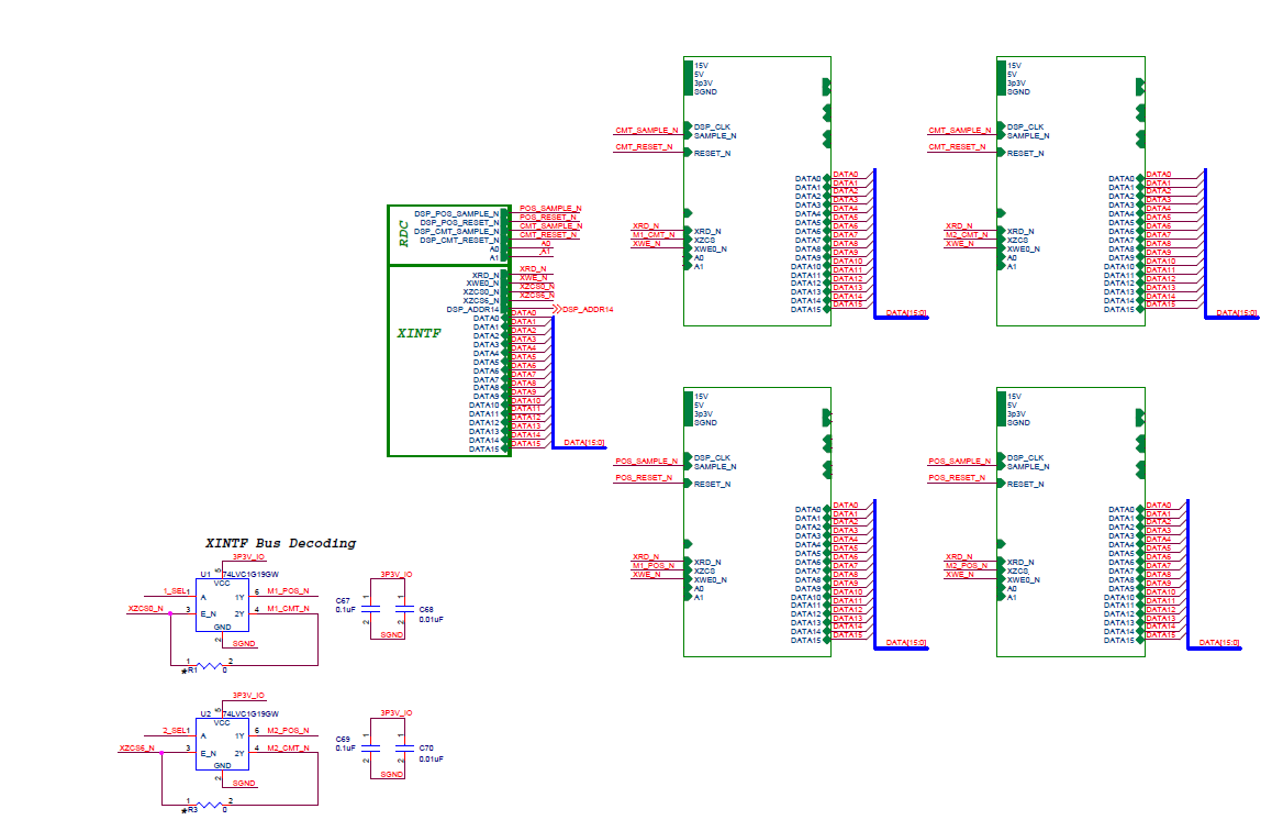
Has anyone tried using a decoder IC to share the parallel bus with multiple devices (sequential access)?  I have 2 of the 3 chip selects available and 4 parallel bus devices to interface with.  My plan was to put 2 on each of the available zones and use a GPIO as a select for the XCSn pin, decoding via SN74LVC1G19.  Pseudo code:

Set_GPIO

ReadRDC1 = *(ZONEn_ADDRESS)

Clear_GPIO

ReadRDC2 = *(ZONEn_ADDRESS)

The decoder will add a delay to the CS edges, but I think that can be compensated for with the lead time parameter, at the cost of a longer overall XINTF acquisition.  With XTIMCLK = SYSCLKOUT, I think I can get away with setting XRDLEAD (and XWRLEAD) to 1 (6.67ns) as the decoder has a max propagation delay of 5.4ns.  To be safe, I'd probably set it to 2.  I also think the delay from de-asserting the chips select should have close to the same effect as putting in a XRDTRAIL value of 1 (i.e. delaying CS wrt to the rest of the bus by 5.4ns).

I would still need to check with setup and hold times on the devices connected to the parallel bus, of course...

Paul

  • Hi Paul,

    I'm afraid the only part that you mentioned that I know anything about is the SN74LVC1G19 (I'm a specialist on Logic, Switches, Multiplexers, and Voltage Translation).

    Can you share a schematic of what you intend to do so I can better understand how these parts communicate/connect?
  • Sure thing.  I've pasted in a partial schematic of what I'm looking to do.  Hopefully you can zoom in and see whats going on.  If not, I'll give a brief description.  The databus is shared between the DSP and the 4 devices on the right.  The read select and write enable are also shared.  The devices we're using do not have an address bus, per se.  There are 2 address pins that are setup before the chip is accessed and we use GPIO for those.  I have Zone 0's chip select going to the E pin on the top decoder and Zone 6's chips select going to the bottom one.  Each decoder has a GPIO select line connected to the 'A' pin.  The top decoders Y1 pin is connected to the bottom left block's (of the 4 blocks on the right) chip select and the Y2 pin goes to the top left block.  The bottom decoder is similarly connected to the right blocks (bottom and top, respectively).  Let me know if you'd like more details.  Thanks!

  • It seems that you have this pretty well worked out. Basically this device just holds one line high while allowing the other one to be driven high or low by the E\ input. The SN74LVC1G19 will add a delay to your signals of between 1.1 and 5.2 ns at a 3.3-V Vcc.

    Have you considered using a switch instead? The SN74LVC1G3157 is an SPDT switch that has a t_pd of ~0.8ns at 3.3-V Vcc.

    If you need additional help with one of our DSP's, I'll have to refer you back to their forum b/c that's way over my head!
  • Hi Emrys.

    I hadn't considered an analog switch, but the low propagation delay is appealing. I actually need a -40(or -55) to 125C part, so that particular one won't work for our application. I looked at ts5a23157-q1, but I'm a little concerned about the break-before-make operation. What would the output chip select's logic state be during that time? Even though it is only about 0.5ns where it is in that state, it's probably better if the output logic is always defined.
  • Usually you don't want to leave an input floating, but in this case I don't think you'll run into any problem.  The input has intrinsic capacitance (usually ~15pF) and then the line is going to be in high impedance mode (1Mohm+) for that ~0.5ns.  Even taking leakages into account, your inputs won't dip much at all under those conditions.  (RC time constant 15pF * 1Mohm = 15us)