Hi,
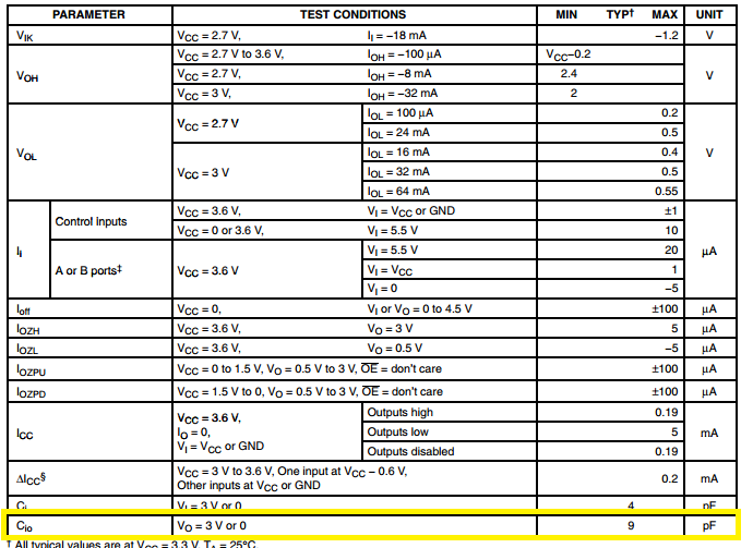
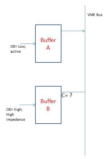
I am using buffers SN74LVT245B and SN74BCT760 for VME interface. Please let me know the input capacitance for these devices when these are in high impedance state ( OE is high ).
Thanks & Regards
Madhu Sharma
Hi,
I am using buffers SN74LVT245B and SN74BCT760 for VME interface. Please let me know the input capacitance for these devices when these are in high impedance state ( OE is high ).
Thanks & Regards
Madhu Sharma