This thread has been locked.

If you have a related question, please click the "Ask a related question" button in the top right corner. The newly created question will be automatically linked to this question.

CD4094B: CD4094B Power Up Waveform

Part Number: CD4094B

Hi team,

  My customer has met an issue with CD4094B during power up. Description is as below:

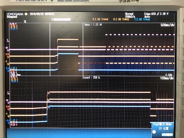
1. CD4094B has control pins of STORBE, DATA, CLOCK, Output enable. All pins are pulled to high during power up. 

2. Customer monitors the output Q1~Q7 pin during power up. Some patch of the boards have H-level output while some are L-level output. All the boards have the same design. 

  Would you help explain if this behavior makes sense and why? Thanks ahead.

,


Regards

Patrick

  • Hi Patrick,

    Any logic register device uses latches to store data.  Latches have an unknown startup state.

    Data must be clocked through to have a valid output state.

  • Hi Emrys,
    Are you saying that either H or L- level output is possible during power up, which is not abnormal behavior?
    In customer's application, they would like to keep outputs low when starting up so what do you suggestion we should implement it? THanks.

    Regards,
    Patrick
  • The best way to achieve this is to use the output enable pin to force the outputs into a high impedance state during power-on, then connect pull-down resistors at each output to force them to a low level. This will ensure that the outputs remain low until data can be clocked through and the OE pin can be deasserted by the controller.
  • Hi Emrys,
    Got it. I can understand the approach to ensure low output during statt-up well. One more thing I need your help to explain:
    Customer has tested 3 different batches of samples, say #1 to #3, while all samples from batch #1 have H output during start-up. All samples from #2, #3 batch have L output during start-up. Question will be, if latches have an unknown startup state, then it should be some probability of H or L within the same batch. It will be strange and difficult to make sense to customer. Could you help clarify here? Thanks.

    Regards,
    Patrick
  • Hello Patrick,

    There's a basic logic building block in any type of shift register or flip flop called a latch.

    Here's one implementation that's commonly seen:

    Now, the question is: what is the value of Q when the system turns on?

    If we assume that R, S, Q, and Q\ are in the LOW state when Vcc = 0V, as Vcc increases from 0V to operating voltage (perhaps 1.8V), eventually the MOSFETs inside these devices will turn on and start to conduct.  With all inputs = 0V, the NOR gates will attempt to drive Q and Q\ HIGH simultaneously. If Q and Q\ go HIGH, then the devices will attempt to drive the outputs LOW.

    This line of thinking is correct, and ends with an oscillator that will never latch until R or S is forced HIGH.

    Unfortunately, this line of thinking is also 'ideal' and doesn't take into account the real world.

    In a real device, there are minor differences in the output driver strengths. There are also differences in internal trace length and layout in the IC.  Even if the latch is designed perfectly, there is external and internal noise that will cause the output to latch to one state or the other.

    We do not design our latched parts to have a default output state.  You _MUST_ clock data through them before the outputs are defined.