Other Parts Discussed in Thread: SN74LVC1G08, SN74LVC14A
This is my CD40109B circuit w/ R26.1 = 4x10K, R25.1-A = 4x100K and Cx.1-.4 = 47pF:
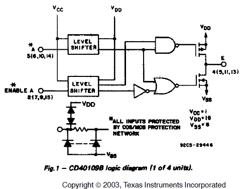
To protect against the Input rising above the Vcc input, I expect that the input protection diode circuit shown in the bottom part of Fig.1 below will suffice assuming the current through the R26 resistor does not exceed the max input current.
However, I have some uncertainties...
a) I assume/expect that the max input current per pin rating from the datasheet
is the rating of the input protection circuit shown at the bottom of the datasheet's Fig.1 (since the figure states "*All inputs protected by COS/MOS protection network"). However, the figure shows the top of the diodes connected to VDD, not VCC. Is this an error, or am I misunderstanding the function/purpose of this figure (or perhaps both are true :) ).
For example, if VCC is a smaller value than VDD, and these inputs are clamped to VDD, then it seems the inputs would have a limited range based on VDD (which doesn't make sense to me based on the level shifting function of the IC).
b) Again with Fig.1, the top portion of the diodes show two diodes connected anode-to-anode; I don't understand what this can protect, unless I assume that these are only protecting when the top diode reaches its reverse voltage rating. If not, how does this circuit protect? If so, what is that voltage rating that it clamps at?
c) Is there any documentation available already that explains these details?
d) The datasheet is an old photocopy with changes (I assume TI obtained this design through the purchase of another company). Will TI create an updated datasheet anytime soon?